Programming Adapter Target Connector Signals
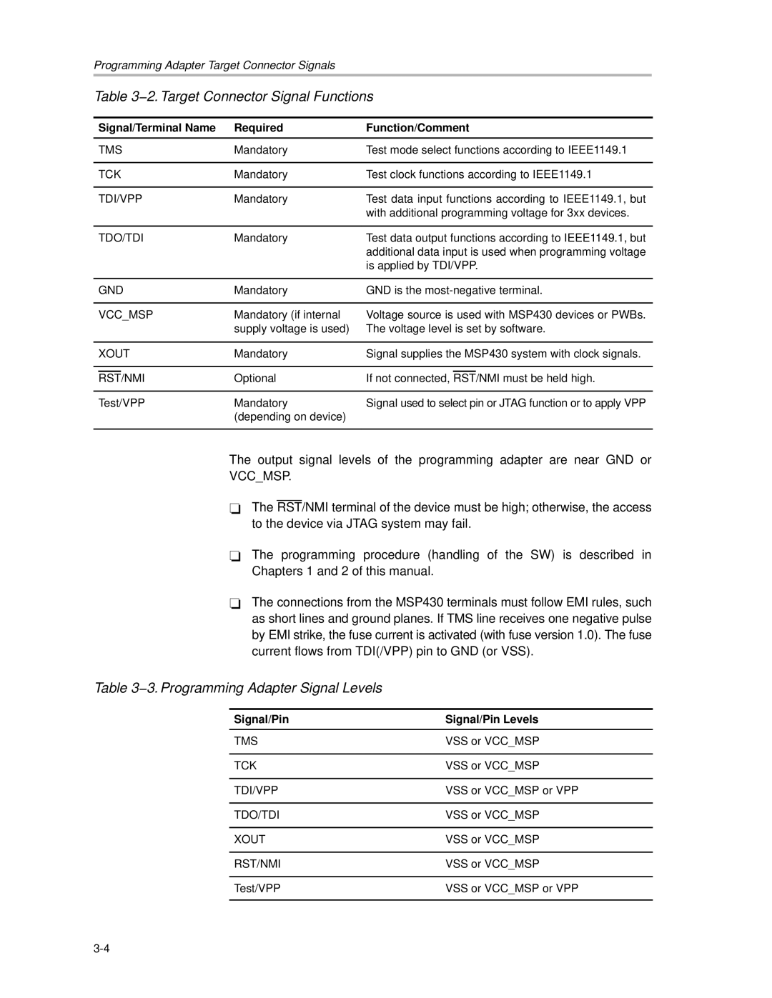
Table 3−2. Target Connector Signal Functions
| Signal/Terminal Name | Required | Function/Comment | |||
| TMS | Mandatory | Test mode select functions according to IEEE1149.1 | |||
|
|
|
|
|
|
|
| TCK | Mandatory | Test clock functions according to IEEE1149.1 | |||
|
|
|
|
|
|
|
| TDI/VPP | Mandatory | Test data input functions according to IEEE1149.1, but | |||
|
|
|
| with additional programming voltage for 3xx devices. | ||
|
|
|
|
|
|
|
| TDO/TDI | Mandatory | Test data output functions according to IEEE1149.1, but | |||
|
|
|
| additional data input is used when programming voltage | ||
|
|
|
| is applied by TDI/VPP. | ||
|
|
|
|
|
|
|
| GND | Mandatory | GND is the | |||
|
|
|
|
|
|
|
| VCC_MSP | Mandatory (if internal | Voltage source is used with MSP430 devices or PWBs. | |||
|
|
| supply voltage is used) | The voltage level is set by software. | ||
|
|
|
|
|
|
|
| XOUT | Mandatory | Signal supplies the MSP430 system with clock signals. | |||
|
|
|
|
|
| |
|
|
| Optional | If not connected, |
|
|
| RST/NMI | RST/NMI must be held high. | ||||
|
|
|
| |||
| Test/VPP | Mandatory | Signal used to select pin or JTAG function or to apply VPP | |||
|
|
| (depending on device) |
|
|
|
|
|
|
|
|
|
|
The output signal levels of the programming adapter are near GND or VCC_MSP.
-The RST/NMI terminal of the device must be high; otherwise, the access to the device via JTAG system may fail.
-The programming procedure (handling of the SW) is described in Chapters 1 and 2 of this manual.
-The connections from the MSP430 terminals must follow EMI rules, such as short lines and ground planes. If TMS line receives one negative pulse by EMI strike, the fuse current is activated (with fuse version 1.0). The fuse current flows from TDI(/VPP) pin to GND (or VSS).
Table 3−3. Programming Adapter Signal Levels
Signal/Pin | Signal/Pin Levels |
TMS | VSS or VCC_MSP |
|
|
TCK | VSS or VCC_MSP |
|
|
TDI/VPP | VSS or VCC_MSP or VPP |
|
|
TDO/TDI | VSS or VCC_MSP |
|
|
XOUT | VSS or VCC_MSP |
|
|
RST/NMI | VSS or VCC_MSP |
|
|
Test/VPP | VSS or VCC_MSP or VPP |
|
|