Interconnection of MSP−PRGS430 to Flash-Based MSP430 Devices
3.7 Interconnection of MSP−PRGS430 to Flash-Based MSP430 Devices
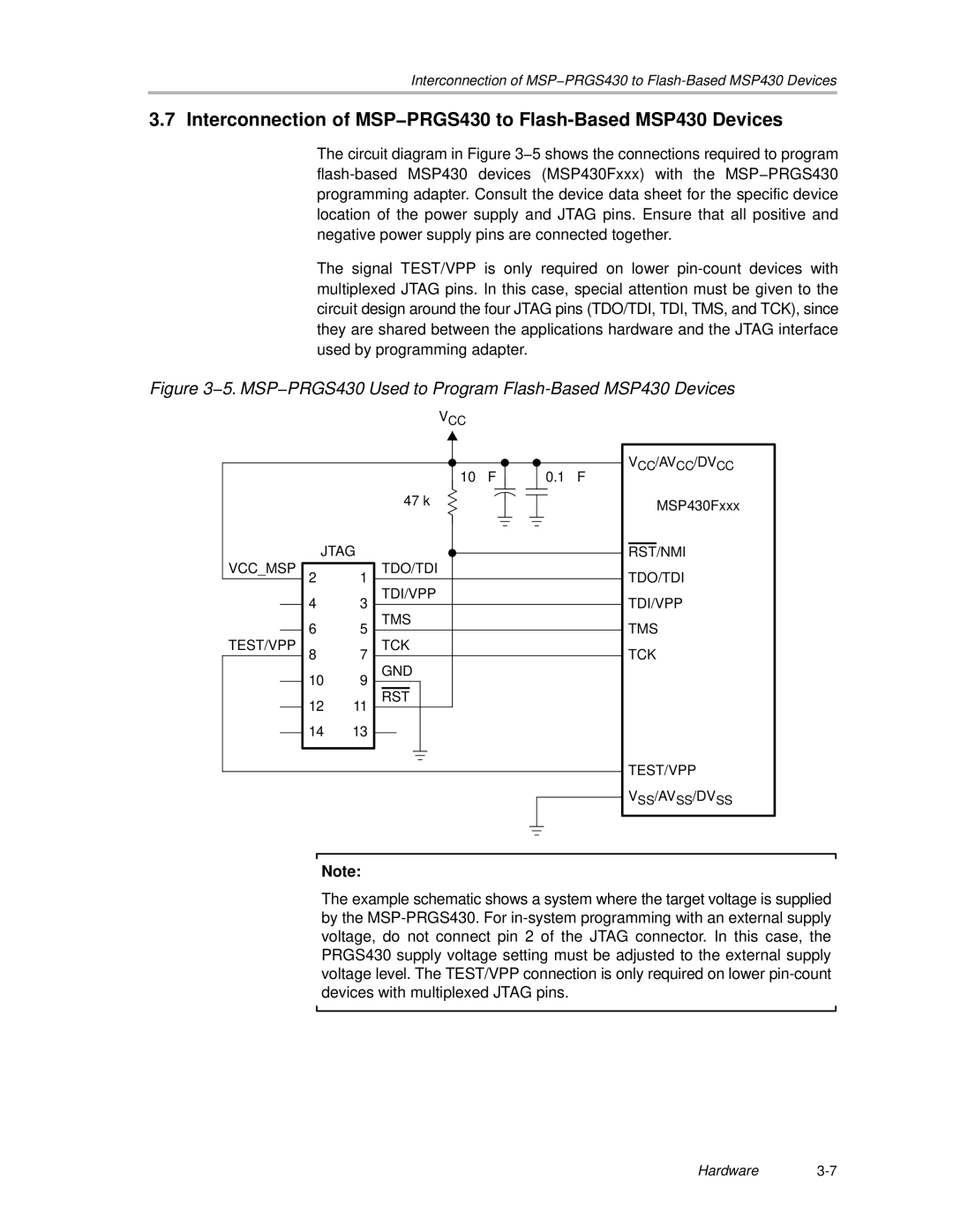
The circuit diagram in Figure 3−5 shows the connections required to program flash-based MSP430 devices (MSP430Fxxx) with the MSP−PRGS430 programming adapter. Consult the device data sheet for the specific device location of the power supply and JTAG pins. Ensure that all positive and negative power supply pins are connected together.
The signal TEST/VPP is only required on lower pin-count devices with multiplexed JTAG pins. In this case, special attention must be given to the circuit design around the four JTAG pins (TDO/TDI, TDI, TMS, and TCK), since they are shared between the applications hardware and the JTAG interface used by programming adapter.
Figure 3−5. MSP−PRGS430 Used to Program Flash-Based MSP430 Devices
| | | VCC | |
| | | 10 ∝F | VCC/AVCC/DVCC |
| | | 0.1 ∝F |
| | | 47 kΩ | MSP430Fxxx |
| | | |
| JTAG | | RST/NMI |
VCC_MSP | 2 | 1 | TDO/TDI | TDO/TDI |
| 4 | 3 | TDI/VPP | TDI/VPP |
| |
| 6 | 5 | TMS | TMS |
| |
TEST/VPP | 8 | 7 | TCK | TCK |
| 10 | 9 | GND | |
| | |
| 12 | 11 | RST | |
| | |
| 14 | 13 | | |
| | | | TEST/VPP |
| | | | VSS/AVSS/DVSS |
| Note: | | |
The example schematic shows a system where the target voltage is supplied by the MSP-PRGS430. For in-system programming with an external supply voltage, do not connect pin 2 of the JTAG connector. In this case, the PRGS430 supply voltage setting must be adjusted to the external supply voltage level. The TEST/VPP connection is only required on lower pin-count devices with multiplexed JTAG pins.