Installation and Configuration
Internal PCB Jumper Selections
the front panel LOCAL switch, control of the OVP trip level changes from software control to the front panel OVP potentiometer. The default OVP trip level is set as 110% of the power supply's rated output voltage. See Table 2.5, on page 22 for a complete list of remote power ON default settings.
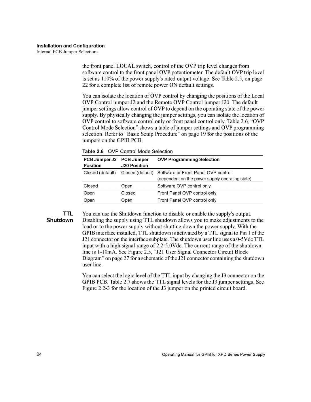
You can isolate the location of OVP control by changing the positions of the Local OVP Control jumper J2 and the Remote OVP Control jumper J20. The default jumper settings allow control of OVP to depend on the operating state of the power supply. By physically changing the jumper settings, you can isolate the location of OVP control to software control only or front panel control only. Table 2.6, “OVP Control Mode Selection” shows a table of jumper settings and OVP programming selection. Refer to “Basic Setup Procedure” on page 19 for the positions of the jumpers on the GPIB PCB.
Table 2.6 OVP Control Mode Selection
PCB Jumper J2 | PCB Jumper | OVP Programming Selection |
Position | J20 Position |
|
Closed (default) | Closed (default) | Software or Front Panel OVP control |
|
| (dependent on the power supply operating state) |
Closed | Open | Software OVP control only |
Open | Closed | Front Panel OVP control only |
Open | Open | Front Panel OVP control only |
TTL You can use the Shutdown function to disable or enable the supply's output. Shutdown Disabling the supply using TTL shutdown allows you to make adjustments to the
load or to the power supply without shutting down the power supply. With the GPIB interface installed, TTL shutdown is activated by a TTL signal to Pin 1 of the J21 connector on the interface subplate. The shutdown user line uses a
You can select the logic level of the TTL input by changing the J3 connector on the GPIB PCB. Table 2.7 shows the TTL signal levels for the J3 jumper settings. See Figure
24 | Operating Manual for GPIB for XPD Series Power Supply |