Overview
R
Implementation Design Overview
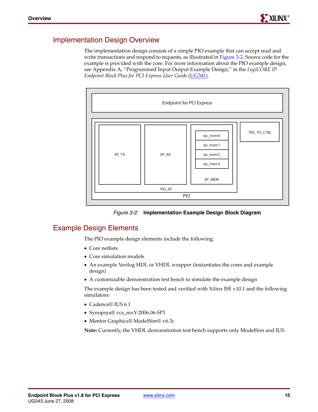
The implementation design consists of a simple PIO example that can accept read and write transactions and respond to requests, as illustrated in Figure
Endpoint for PCI Express
|
|
|
|
|
|
|
|
|
|
|
|
|
|
|
|
|
|
|
|
|
|
|
|
|
|
|
|
| PIO_TO_CTRL |
|
|
|
|
|
|
|
|
|
|
|
|
|
|
|
|
| |
|
|
|
|
|
|
|
|
| ep_mem0 |
|
|
|
|
| |
|
|
|
|
|
|
|
|
|
|
|
|
|
|
| |
|
|
|
|
|
|
|
|
|
|
|
|
|
|
|
|
|
|
|
|
|
|
|
|
| ep_mem1 |
|
|
|
|
|
|
|
|
|
|
|
|
|
|
|
|
|
|
| |||
|
|
| EP_TX |
| EP_RX |
|
|
|
|
|
|
|
| ||
|
|
|
|
|
|
| ep_mem2 |
|
|
|
|
|
| ||
|
|
|
|
|
|
|
|
|
|
|
|
|
| ||
|
|
|
|
|
|
|
|
| ep_mem3 |
|
|
|
|
|
|
|
|
|
|
|
|
|
|
|
|
|
|
|
| ||
|
|
|
|
|
|
|
|
| EP_MEM |
|
|
|
|
| |
|
|
|
|
|
|
|
|
|
|
|
|
|
|
|
|
|
|
|
|
| PIO_EP |
|
|
|
|
|
|
|
|
|
|
|
|
|
|
|
|
|
|
|
|
|
|
|
| ||
|
|
|
|
|
| PIO |
| ||||||||
|
|
|
|
|
|
|
|
|
|
|
|
|
|
| |
|
|
|
|
|
|
|
|
|
|
|
|
|
|
|
|
|
|
| Figure | ||||||||||||
Example Design Elements
The PIO example design elements include the following:
•Core netlists
•Core simulation models
•An example Verilog HDL or VHDL wrapper (instantiates the cores and example design)
•A customizable demonstration test bench to simulate the example design
The example design has been tested and verified with Xilinx ISE v10.1 and the following simulators:
•Cadence® IUS 6.1
•Synopsys®
•Mentor Graphics® ModelSim® v6.3c
Note: Currently, the VHDL demonstration test bench supports only ModelSim and IUS.
Endpoint Block Plus v1.8 for PCI Express | www.xilinx.com | 15 |
UG343 June 27, 2008