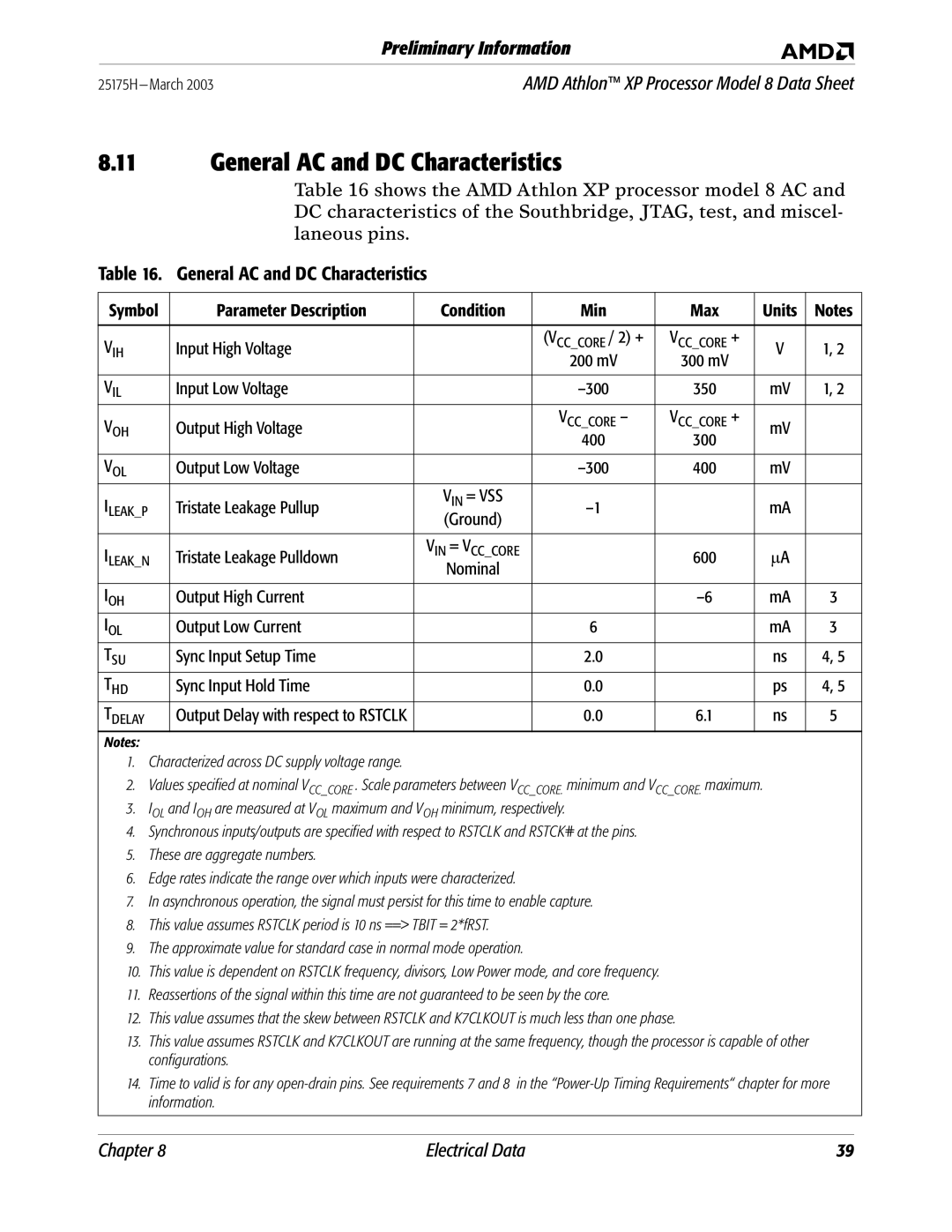
8 specifications
AMD's Ryzen 8000 series, commonly referred to as AMD 8, represents a significant leap in performance and efficiency, leveraging advanced technologies that cater to gamers, content creators, and enterprise users alike. With a continued focus on the Zen architecture, the Ryzen 8000 processors enhance performance per watt, delivering increased efficiency without compromising on power.One of the standout features of AMD 8 is its adoption of the 5nm process technology. This innovation allows for a higher density of transistors, resulting in improved performance metrics and reduced power consumption. The smaller node size not only enhances clock speeds but also ensures that the chips generate less heat, making thermal management easier for system builders.
AMD has introduced a new architecture with the Ryzen 8000 series known as Zen 5. This architecture brings improved instructions per cycle (IPC) over its predecessors, leading to faster performance in both single-threaded and multi-threaded workloads. Gamers will benefit from higher frame rates, while professionals in fields such as video editing and 3D rendering can expect noticeable improvements in rendering times.
Another key technology in the AMD 8 lineup is the integration of AMD's next-generation RDNA graphics architecture. This allows for enhanced graphics performance in systems without dedicated GPU hardware. The combination of advanced graphics and CPU capabilities provides a more versatile platform for casual gamers and users with less demanding graphical needs.
Support for PCIe 5.0 is a game changer for the AMD 8000 series, offering double the bandwidth of its predecessor, PCIe 4.0. This feature allows for faster data transfer rates with compatible SSDs and graphics cards, ensuring that users can take full advantage of the latest storage technologies.
Additionally, AMD's Infinity Cache has made its way into the Ryzen 8000 series, further enhancing memory bandwidth. This technology reduces latency and increases efficiency by caching frequently accessed data closer to the processor.
In terms of connectivity, the Ryzen 8000 models come equipped with Wi-Fi 7 and Bluetooth 5.2, providing ultra-fast wireless connections that are essential for modern gaming and streaming experiences.
In summary, AMD's Ryzen 8000 series, or AMD 8, is designed for maximum performance and efficiency. With its advanced 5nm technology, enhanced Zen 5 architecture, integrated RDNA graphics, PCIe 5.0 support, Infinity Cache, and state-of-the-art connectivity features, it sets a new standard for processors in its class, making it a top choice for both gamers and professionals.