Contents
Cypress Semiconductor Corporation 198 Champion Court
Functional Description
Product Selection Guide Density Mbit 32K x 64K x 128K x
176TQFP 172FBGA
Mirror Reg
Logic Block Diagram
True
RAM Array
Ball BGA Top View
Pin Configurations
CY7C0853AV
CY7C0850AV CY7C0851AV CY7C0852AV
Pin Definitions
Operation Description
Master Reset
Mailbox Interrupts
Address Counter and Mask Register Operations
Mask Load Operation
Mask Reset Operation
Counter Interrupt
Retransmit
CLK
Cnten ADS Cntrst Mrst
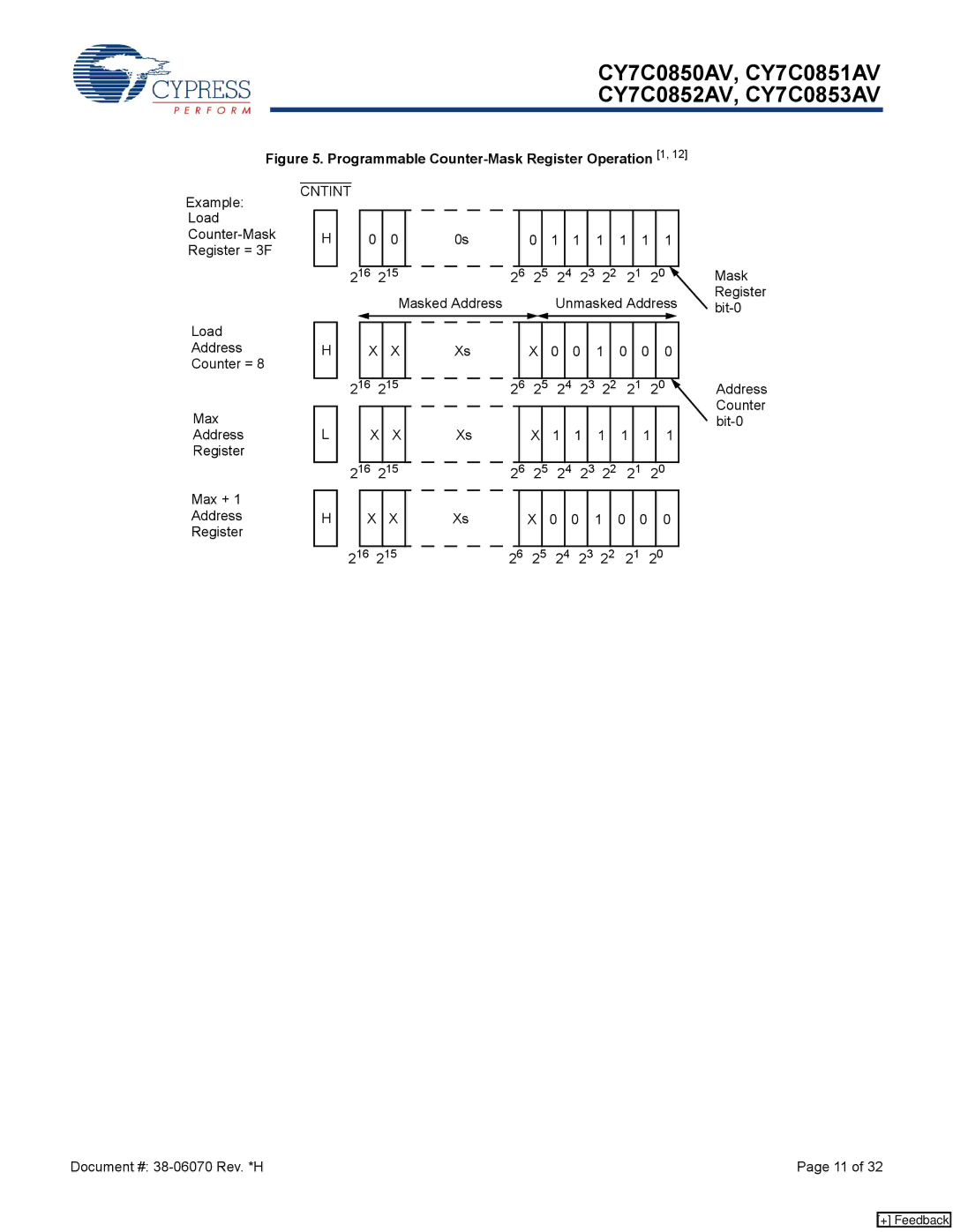
Programmable Counter-Mask Register Operation 1
Ieee 1149.1 Serial Boundary Scan Jtag
Performing a TAP Reset
Capacitance
Electrical Characteristics
Maximum Ratings
Operating Range
Normal Load Load Three-state Delay Load
Switching Characteristics
Master Reset Timing
Port to Port Delays
Parameter Description 167/133/100 Unit Min
Jtag Timing
Master Reset
Switching Waveforms
Bank Select Read 26
Read-to-Write-to-Read OE Controlled 25, 28, 30
Write with Address Counter Advance
Disabled-to-Write-to-Read-to-Write-to-Read
Read-to-Readback-to-Read-to-Read R/W = High
Counter Reset 32
Readback State of Address Counter or Mask Register35, 36, 37
LeftPort LPort Write to RightPort RPort Read39, 40
Counter Interrupt and Retransmit 34, 42, 43, 44
CLK
64K × 36 2M 3.3V Synchronous CY7C0851AV Dual-Port Sram
Ordering Information
256K × 36 9M 3.3V Synchronous CY7C0853AV Dual-Port Sram
128K × 36 4M 3.3V Synchronous CY7C0852AV Dual-Port Sram
Ball Fbga 15 x 15 x 1.25 mm
Package Diagrams
Pin Thin Quad Flat Pack 24 × 24 × 1.4 mm
Submis Orig. Description of Change Sion Date
Document History
USB
Sales, Solutions, and Legal Information
Worldwide Sales and Design Support Products PSoC Solutions

