CY7C1370DV25
CY7C1372DV25
Features
•
•Supports
—Available speed grades are 250, 200 and 167 MHz
•Internally
•Fully registered (inputs and outputs) for pipelined operation
•Byte Write capability
•Single 2.5V core power supply (VDD)
•2.5V I/O power supply (VDDQ)
•Fast
—2.6 ns (for
•Clock Enable (CEN) pin to suspend operation
•Synchronous
•Available in
•IEEE 1149.1
•Burst
•“ZZ” Sleep Mode option and Stop Clock option
Functional Description
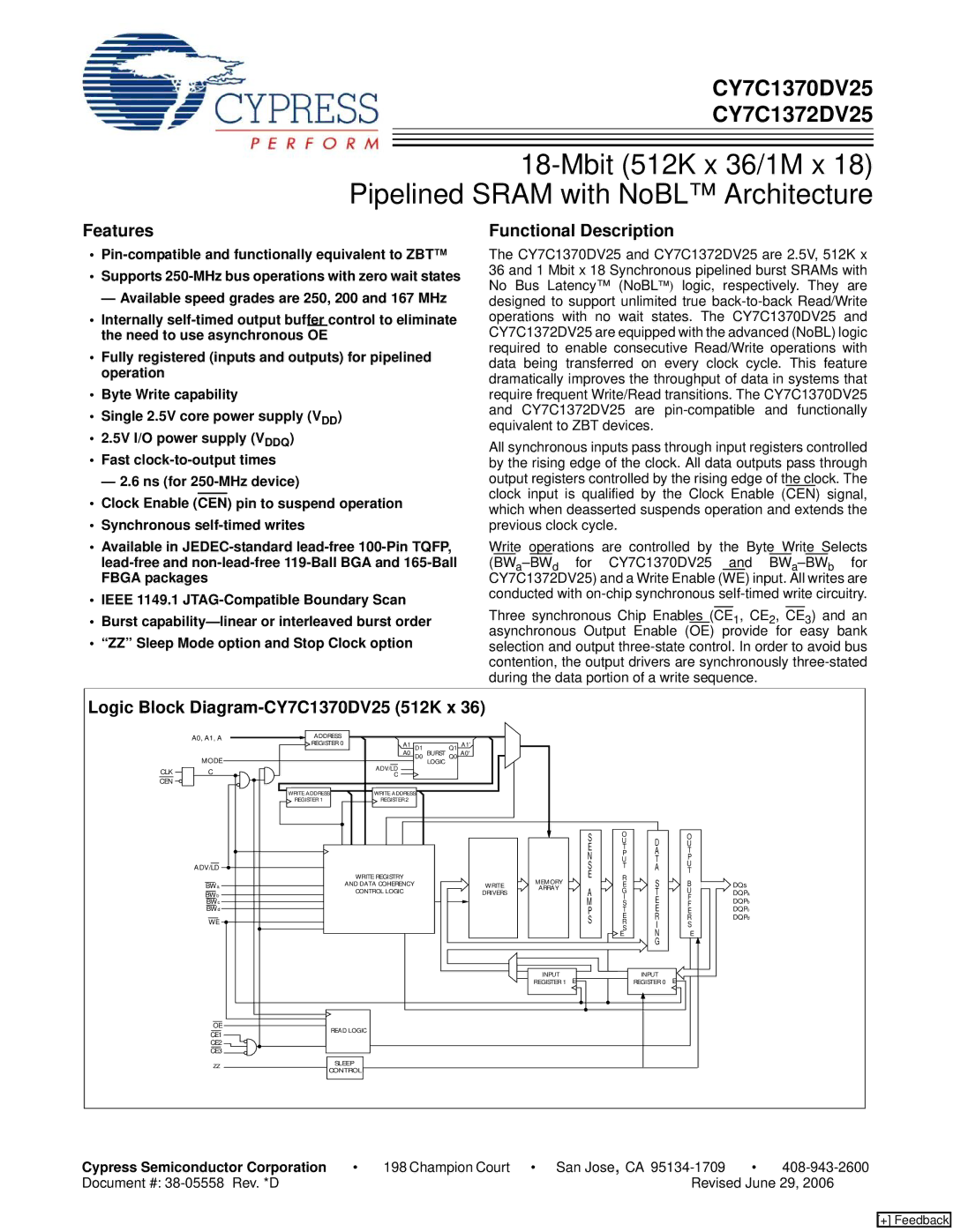
The CY7C1370DV25 and CY7C1372DV25 are 2.5V, 512K x 36 and 1 Mbit x 18 Synchronous pipelined burst SRAMs with No Bus Latency™ (NoBL™) logic, respectively. They are designed to support unlimited true
All synchronous inputs pass through input registers controlled by the rising edge of the clock. All data outputs pass through output registers controlled by the rising edge of the clock. The clock input is qualified by the Clock Enable (CEN) signal, which when deasserted suspends operation and extends the previous clock cycle.
Write operations are controlled by the Byte Write Selects
Three synchronous Chip Enables (CE1, CE2, CE3) and an asynchronous Output Enable (OE) provide for easy bank selection and output
Logic Block |
|
|
|
|
|
|
|
| ||||||
| A0, A1, A | ADDRESS |
|
|
|
|
|
|
|
|
|
|
|
|
|
| REGISTER 0 |
| A1 | D1 | Q1 A1' |
|
|
|
|
|
|
|
|
| MODE |
|
| A0 | D0 BURST Q0 A0' |
|
|
|
|
|
|
|
| |
|
|
| ADV/LD |
| LOGIC |
|
|
|
|
|
|
|
| |
CLK | C |
|
|
|
|
|
|
|
|
|
|
|
| |
|
| C |
|
|
|
|
|
|
|
|
|
| ||
CEN |
|
|
|
|
|
|
|
|
|
|
|
|
| |
|
|
|
|
|
|
|
|
|
|
|
|
|
| |
|
| WRITE ADDRESS |
| WRITE ADDRESS |
|
|
|
|
|
|
|
|
| |
|
| REGISTER 1 |
| REGISTER 2 |
|
|
|
|
|
|
|
|
|
|
|
|
|
|
|
|
|
|
| S | O |
| O |
|
|
|
|
|
|
|
|
|
|
| U | D |
|
| ||
|
|
|
|
|
|
|
|
| E | T | U |
|
| |
|
|
|
|
|
|
|
|
| P | A | T |
|
| |
|
|
|
|
|
|
|
|
| N |
|
| |||
|
|
|
|
|
|
|
|
| U | T | P |
|
| |
| ADV/LD |
|
|
|
|
|
|
| S | T | A | U |
|
|
|
|
|
|
|
|
|
| R | T |
|
| |||
|
|
| WRITE REGISTRY |
|
| MEMORY | E | S | B |
|
| |||
| BWa |
| AND DATA COHERENCY |
| WRITE |
| E | DQs |
| |||||
|
|
|
| ARRAY |
|
| ||||||||
| BWb |
| CONTROL LOGIC |
| DRIVERS |
| A | G | T | U | DQPa |
| ||
|
|
|
|
|
|
| I | F |
| |||||
| BWc |
|
|
|
|
|
|
| M | S | E | DQPb |
| |
|
|
|
|
|
|
|
| F |
| |||||
| BWd |
|
|
|
|
|
|
| P | T | E | E | DQPc |
|
|
|
|
|
|
|
|
|
| E |
| ||||
| WE |
|
|
|
|
|
|
| S | R | R | R | DQPd |
|
|
|
|
|
|
|
|
|
|
| S | I | S |
|
|
|
|
|
|
|
|
|
|
|
| E | N | E |
|
|
|
|
|
|
|
|
|
|
|
|
| G |
|
|
|
|
|
|
|
|
|
|
| INPUT | E |
| INPUT | E |
|
|
|
|
|
|
|
|
| REGISTER 1 |
| REGISTER 0 |
|
| |||
| OE | READ LOGIC |
|
|
|
|
|
|
|
|
|
|
| |
| CE1 |
|
|
|
|
|
|
|
|
|
|
| ||
|
|
|
|
|
|
|
|
|
|
|
|
|
| |
| CE2 |
|
|
|
|
|
|
|
|
|
|
|
|
|
| CE3 |
|
|
|
|
|
|
|
|
|
|
|
|
|
| ZZ | SLEEP |
|
|
|
|
|
|
|
|
|
|
| |
| CONTROL |
|
|
|
|
|
|
|
|
|
|
| ||
|
|
|
|
|
|
|
|
|
|
|
|
| ||
Cypress Semiconductor Corporation | • | 198 Champion Court | • | San Jose, CA | • | |||||||||
Document #: |
|
|
|
|
|
|
|
|
|
| Revised June 29, 2006 | |||
[+] Feedback