CY7C1370DV25
CY7C1372DV25
Document #: 38-05558 Rev. *D Page 12 of 27
BYPASS
When the BYPASS instruction is loaded in the instruction
register and the TAP is placed in a Shift-DR state, the bypass
register is placed between the TDI and TDO balls. The
advantage of the BYPASS instruction is that it shortens the
boundary scan path when multiple devices are connected
together on a board.
EXTEST Output Bus Tri-State
IEEE Standard 1149.1 mandates that the TAP controller be
able to put the output bus into a tri-state mode.
The boundary scan register has a special bit located at bit #85
(for 119-BGA package) or bit #89 (for 165-fBGA package).
When this scan cell, called the “extest output bus tri-state,” is
latched into the preload register during the “Update-DR” state
in the TAP controller, it will directly control the state of the
output (Q-bus) pins, when the EXTEST is entered as the
current instruction. When HIGH, it will enable the output
buffers to drive the output bus. When LOW, this bit will place
the output bus into a High-Z condition.
This bit can be set by entering the SAMPLE/PRELOAD or
EXTEST command, and then shifting the desired bit into that
cell, during the “Shift-DR” state. During “Update-DR,” the value
loaded into that shift-register cell will latch into the preload
register. When the EXTEST instruction is entered, this bit will
directly control the output Q-bus pins. Note that this bit is
preset HIGH to enable the output when the device is
powered-up, and also when the TAP controller is in the
“Test-Logic-Reset” state.
Reserved
These instructions are not implemented but are reserved for
future use. Do not use these instructions.
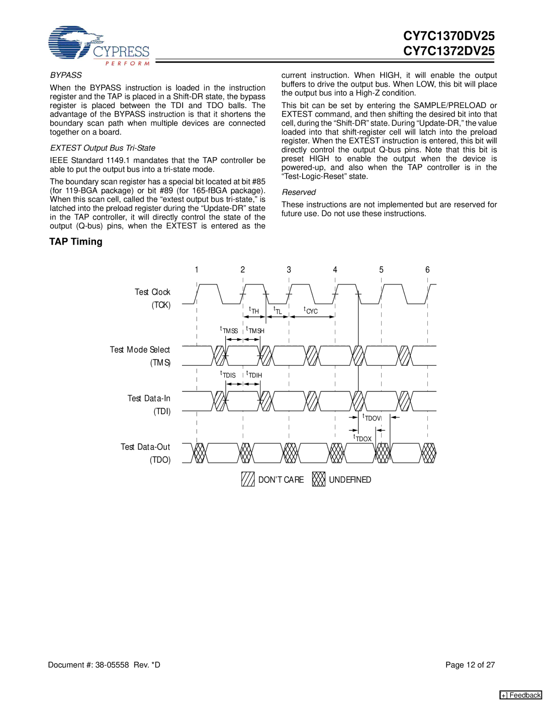
TAP Ti min g
tTL
Test Clock
(TCK)
123456
T
est Mode Select
(TMS)
tTH
Test Data-Out
(TDO)
tCYC
Test Data-In
(TDI)
tTMSH
tTMSS
tTDIH
tTDIS
tTDOX
tTDOV
DON’T CARE UNDEFINED
[+] Feedback