CY7C1370DV25
CY7C1372DV25
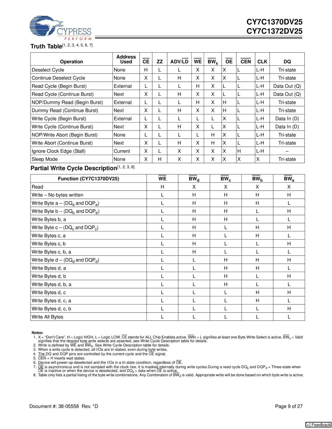
Truth Table[1, 2, 3, 4, 5, 6, 7]
| Address |
|
|
|
|
|
|
|
|
|
|
|
|
|
|
|
|
|
|
|
|
|
|
|
|
|
|
|
|
|
|
|
|
|
|
|
Operation | Used |
| CE |
| ZZ | ADV/LD |
|
| WE |
| BWx |
|
| OE |
|
| CEN |
| CLK |
| DQ | |||||||||||||||
Deselect Cycle | None |
| H |
| L | L |
|
| X |
|
| X |
| X |
| L |
|
| ||||||||||||||||||
Continue Deselect Cycle | None |
| X |
| L | H |
|
| X |
|
| X |
| X |
| L |
|
| ||||||||||||||||||
Read Cycle (Begin Burst) | External |
| L |
| L | L |
|
| H |
|
| X |
| L |
| L |
|
| Data Out (Q) | |||||||||||||||||
Read Cycle (Continue Burst) | Next |
| X |
| L | H |
|
| X |
|
| X |
| L |
| L |
|
| Data Out (Q) | |||||||||||||||||
NOP/Dummy Read (Begin Burst) | External |
| L |
| L | L |
|
| H |
|
| X |
| H |
| L |
|
| ||||||||||||||||||
Dummy Read (Continue Burst) | Next |
| X |
| L | H |
|
| X |
|
| X |
| H |
| L |
|
| ||||||||||||||||||
Write Cycle (Begin Burst) | External |
| L |
| L | L |
|
| L |
|
| L |
| X |
| L |
|
| Data In (D) | |||||||||||||||||
Write Cycle (Continue Burst) | Next |
| X |
| L | H |
|
| X |
|
| L |
| X |
| L |
|
| Data In (D) | |||||||||||||||||
NOP/Write Abort (Begin Burst) | None |
| L |
| L | L |
|
| L |
|
| H |
| X |
| L |
|
| ||||||||||||||||||
Write Abort (Continue Burst) | Next |
| X |
| L | H |
|
| X |
|
| H |
| X |
| L |
|
| ||||||||||||||||||
Ignore Clock Edge (Stall) | Current |
| X |
| L | X |
|
| X |
|
| X |
| X |
| H |
|
|
| – | ||||||||||||||||
Sleep Mode | None |
| X |
| H | X |
|
| X |
|
| X |
| X |
| X |
| X |
| |||||||||||||||||
Partial Write Cycle Description[1, 2, 3, 8] |
|
|
|
|
|
|
|
|
|
|
|
|
|
|
|
|
|
|
|
|
|
|
|
|
|
|
|
|
|
|
|
|
|
| ||
Function (CY7C1370DV25) |
|
|
|
| WE |
|
|
|
| BW | d |
|
|
| BW | c |
|
|
|
|
| BW | b |
|
| BW | a | |||||||||
Read |
|
|
|
|
|
| H |
|
|
|
| X |
|
|
|
| X |
|
|
|
|
|
| X |
|
| X | |||||||||
Write – No bytes written |
|
|
|
|
|
| L |
|
|
|
| H |
|
|
|
| H |
|
|
|
|
|
| H |
|
| H | |||||||||
Write Byte a – (DQa and DQPa) |
|
|
|
|
|
| L |
|
|
|
| H |
|
|
|
| H |
|
|
|
|
|
| H |
|
| L | |||||||||
Write Byte b – (DQb and DQPb) |
|
|
|
|
|
| L |
|
|
|
| H |
|
|
|
| H |
|
|
|
|
|
| L |
|
| H | |||||||||
Write Bytes b, a |
|
|
|
|
|
| L |
|
|
|
| H |
|
|
|
| H |
|
|
|
|
|
| L |
|
| L | |||||||||
Write Byte c – (DQc and DQPc) |
|
|
|
|
|
| L |
|
|
|
| H |
|
|
|
| L |
|
|
|
|
|
| H |
|
| H | |||||||||
Write Bytes c, a |
|
|
|
|
|
| L |
|
|
|
| H |
|
|
|
| L |
|
|
|
|
|
| H |
|
| L | |||||||||
Write Bytes c, b |
|
|
|
|
|
| L |
|
|
|
| H |
|
|
|
| L |
|
|
|
|
|
| L |
|
| H | |||||||||
Write Bytes c, b, a |
|
|
|
|
|
| L |
|
|
|
| H |
|
|
|
| L |
|
|
|
|
|
| L |
|
| L | |||||||||
Write Byte d – (DQd and DQPd) |
|
|
|
|
|
| L |
|
|
|
| L |
|
|
|
| H |
|
|
|
|
|
| H |
|
| H | |||||||||
Write Bytes d, a |
|
|
|
|
|
| L |
|
|
|
| L |
|
|
|
| H |
|
|
|
|
|
| H |
|
| L | |||||||||
Write Bytes d, b |
|
|
|
|
|
| L |
|
|
|
| L |
|
|
|
| H |
|
|
|
|
|
| L |
|
| H | |||||||||
Write Bytes d, b, a |
|
|
|
|
|
| L |
|
|
|
| L |
|
|
|
| H |
|
|
|
|
|
| L |
|
| L | |||||||||
Write Bytes d, c |
|
|
|
|
|
| L |
|
|
|
| L |
|
|
|
| L |
|
|
|
|
|
| H |
|
| H | |||||||||
Write Bytes d, c, a |
|
|
|
|
|
| L |
|
|
|
| L |
|
|
|
| L |
|
|
|
|
|
| H |
|
| L | |||||||||
Write Bytes d, c, b |
|
|
|
|
|
| L |
|
|
|
| L |
|
|
|
| L |
|
|
|
|
|
| L |
|
| H | |||||||||
Write All Bytes |
|
|
|
|
|
| L |
|
|
|
| L |
|
|
|
| L |
|
|
|
|
|
| L |
|
| L | |||||||||
Notes:
1.X = “Don't Care”, H = Logic HIGH, L = Logic LOW, CE stands for ALL Chip Enables active. BWx = L signifies at least one Byte Write Select is active, BWx = Valid signifies that the desired byte write selects are asserted, see Write Cycle Description table for details.
2.Write is defined by WE and BWX. See Write Cycle Description table for details.
3.When a write cycle is detected, all I/Os are
4.The DQ and DQP pins are controlled by the current cycle and the OE signal.
5.CEN = H inserts wait states.
6.Device will
7.OE is asynchronous and is not sampled with the clock rise. It is masked internally during write cycles.During a read cycle DQs and DQPX =
8.Table only lists a partial listing of the byte write combinations. Any Combination of BWX is valid. Appropriate write will be done based on which byte write is active.
Document #: | Page 9 of 27 |
[+] Feedback