Manuals
/
Cypress
/
Computer Equipment
/
Computer Hardware
Cypress
CY7C1372DV25, CY7C1370DV25
manual
Ball BGA 14 x 22 x 2.4 mm
Models:
CY7C1372DV25
CY7C1370DV25
1
25
27
27
Download
27 pages
34.5 Kb
20
21
22
23
24
25
26
27
TAP Controller State Diagram
Features
Switching Waveforms
ZZ Mode Timing28
Page 25
Image 25
CY7C1370DV25
CY7C1372DV25
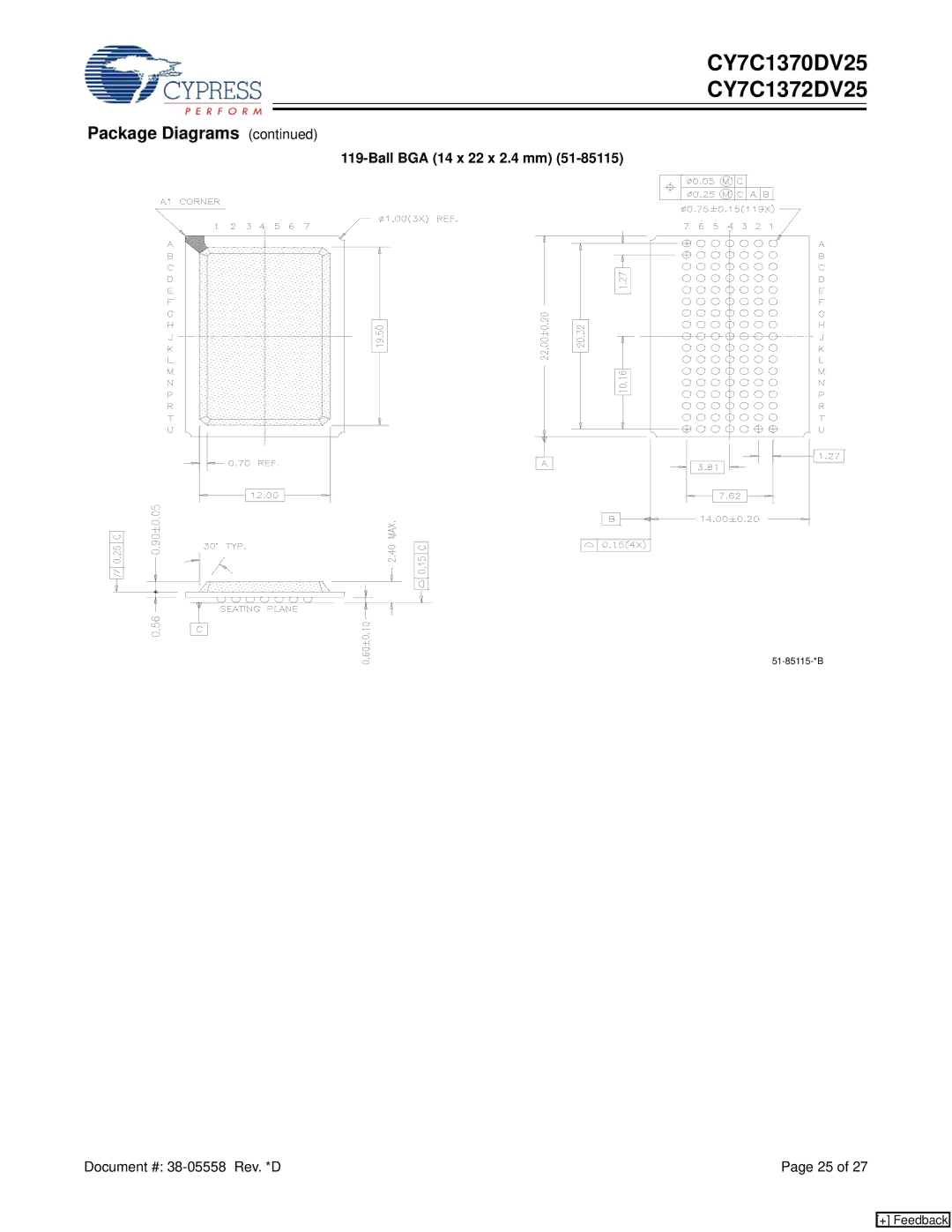
Package Diagrams
(continued)
119-Ball
BGA (14 x 22 x 2.4 mm)
(51-85115)
51-85115-*B
Document #:
38-05558
Rev. *D
Page 25 of 27
[+] Feedback
Page 24
Page 26
Page 25
Image 25
Page 24
Page 26
Contents
Logic Block Diagram-CY7C1370DV25 512K x
Features
Functional Description
Cypress Semiconductor Corporation
Selection Guide
Logic Block Diagram-CY7C1372DV25 1M x
250 MHz 200 MHz 167 MHz Unit
1M ×
Pin Configurations Pin Tqfp Pinout
CY7C1370DV25 512K ×
Pin Configurations Ball BGA Pinout
Pin Configurations Ball Fbga Pinout
Pin Name Type Pin Description
Pin Definitions
Byte Write Select Inputs, active LOW. Qualified with
Clock input to the Jtag circuitry
Introduction
Linear Burst Address Table Mode = GND
Interleaved Burst Address Table Mode = Floating or VDD
ZZ Mode Electrical Characteristics
Address Operation Used
Partial Write Cycle Description 1, 2, 3
Function CY7C1370DV25
TAP Controller Block Diagram
TAP Controller State Diagram
Ieee 1149.1 Serial Boundary Scan Jtag
TAP Instruction Set
TAP Registers
Bypass
TAP Timing
Parameter Description Min Max Unit Clock
TAP AC Switching Characteristics Over the Operating Range9
Output Times
Hold Times
5V TAP AC Test Conditions
TAP DC Electrical Characteristics And Operating Conditions
5V TAP AC Output Load Equivalent
Scan Register Sizes
Ball BGA Boundary Scan Order 12
Identification Codes
Instruction Code Description
Bit # Ball ID
Ball Fbga Boundary Scan Order 12
Maximum Ratings
Electrical Characteristics Over the Operating Range15
Operating Range
Range Ambient
Thermal Resistance17
Capacitance17
AC Test Loads and Waveforms
Package
250 200 167 Parameter Description Unit Min Max
Switching Characteristics Over the Operating Range 22
Set-up Times
Read/Write/Timing24, 25
Switching Waveforms
Address A1 A2
DON’T Care
NOP,STALL and Deselect Cycles24, 25
ZZ Mode Timing28
Ordering Information
CY7C1370DV25 CY7C1372DV25
Pin Thin Plastic Quad Flatpack 14 x 20 x 1.4 mm
Package Diagrams
Ball BGA 14 x 22 x 2.4 mm
Ball Fbga 13 x 15 x 1.4 mm
Document History
ECN No Issue Date Orig. Description of Change
Top
Page
Image
Contents