CY7C1370DV25
CY7C1372DV25
signals. The CY7C1370DV25/CY7C1372DV25 provides byte write capability that is described in the Write Cycle Description table. Asserting the Write Enable input (WE) with the selected Byte Write Select (BW) input will selectively write to only the desired bytes. Bytes not selected during a byte write operation will remain unaltered. A synchronous
Because the CY7C1370DV25 and CY7C1372DV25 are common I/O devices, data should not be driven into the device while the outputs are active. The Output Enable (OE) can be deasserted HIGH before presenting data to the DQ and DQP (DQa,b,c,d/DQPa,b,c,d for CY7C1370DV25 and DQa,b/DQPa,b for CY7C1372DV25) inputs. Doing so will
Burst Write Accesses
The CY7C1370DV25/CY7C1372DV25 has an
Sleep Mode
The ZZ input pin is an asynchronous input. Asserting ZZ places the SRAM in a power conservation “sleep” mode. Two clock cycles are required to enter into or exit from this “sleep” mode. While in this mode, data integrity is guaranteed. Accesses pending when entering the “sleep” mode are not considered valid nor is the completion of the operation guaranteed. The device must be deselected prior to entering the “sleep” mode. CE1, CE2, and CE3, must remain inactive for the duration of tZZREC after the ZZ input returns LOW.
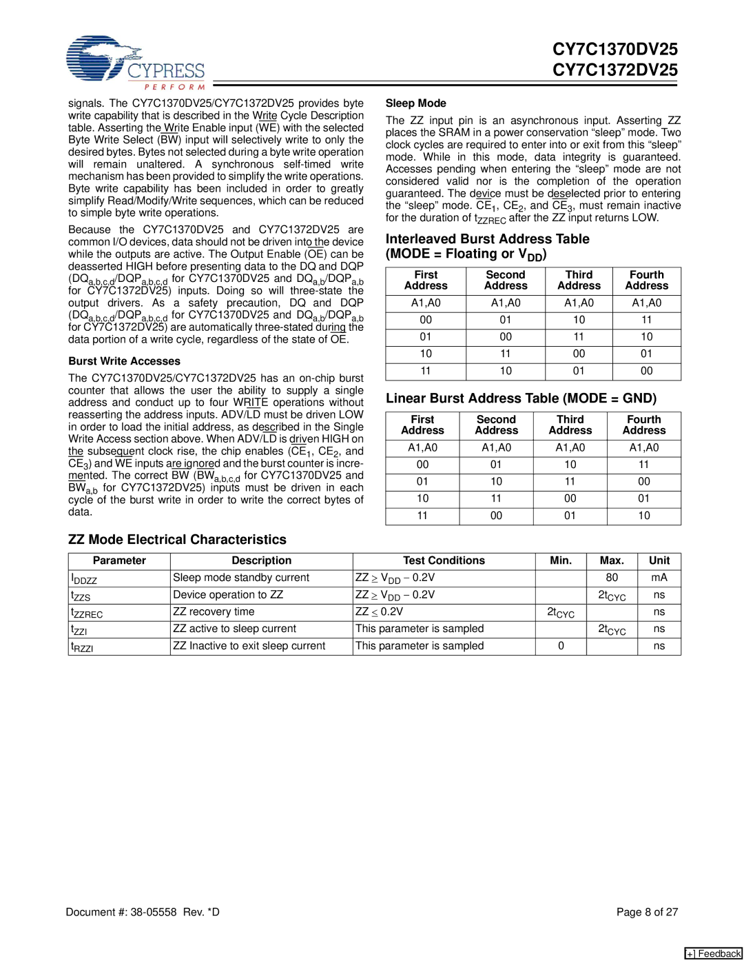
Interleaved Burst Address Table (MODE = Floating or VDD)
First | Second | Third | Fourth |
Address | Address | Address | Address |
|
|
|
|
A1,A0 | A1,A0 | A1,A0 | A1,A0 |
|
|
|
|
00 | 01 | 10 | 11 |
|
|
|
|
01 | 00 | 11 | 10 |
|
|
|
|
10 | 11 | 00 | 01 |
|
|
|
|
11 | 10 | 01 | 00 |
|
|
|
|
Linear Burst Address Table (MODE = GND)
First | Second | Third | Fourth |
Address | Address | Address | Address |
|
|
|
|
A1,A0 | A1,A0 | A1,A0 | A1,A0 |
|
|
|
|
00 | 01 | 10 | 11 |
|
|
|
|
01 | 10 | 11 | 00 |
|
|
|
|
10 | 11 | 00 | 01 |
|
|
|
|
11 | 00 | 01 | 10 |
|
|
|
|
ZZ Mode Electrical Characteristics
Parameter | Description | Test Conditions | Min. | Max. | Unit |
IDDZZ | Sleep mode standby current | ZZ > VDD − 0.2V |
| 80 | mA |
tZZS | Device operation to ZZ | ZZ > VDD − 0.2V |
| 2tCYC | ns |
tZZREC | ZZ recovery time | ZZ < 0.2V | 2tCYC |
| ns |
tZZI | ZZ active to sleep current | This parameter is sampled |
| 2tCYC | ns |
tRZZI | ZZ Inactive to exit sleep current | This parameter is sampled | 0 |
| ns |
Document #: | Page 8 of 27 |
[+] Feedback