CY7C1380DV25, CY7C1380FV25 CY7C1382DV25, CY7C1382FV25

IEEE 1149.1 Serial Boundary Scan (JTAG)

The CY7C1380DV25/CY7C1382DV25 incorporates a serial boundary scan test access port (TAP). This part is fully compliant with 1149.1. The TAP operates using JEDEC-standard 3.3V or 2.5V IO logic levels.

The CY7C1380DV25/CY7C1382DV25 contains a TAP controller, instruction register, boundary scan register, bypass register, and ID register.

Disabling the JTAG Feature

It is possible to operate the SRAM without using the JTAG feature. To disable the TAP controller, TCK must be tied LOW (VSS) to prevent clocking of the device. TDI and TMS are internally pulled up and may be unconnected. They may alternately be connected to VDD through a pull up resistor. TDO must be left unconnected. Upon power up, the device will come up in a reset state which will not interfere with the operation of the device.

TAP Controller State Diagram

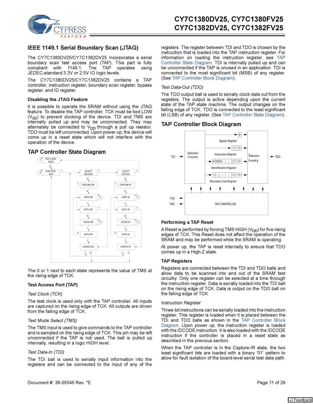
registers. The register between TDI and TDO is chosen by the instruction that is loaded into the TAP instruction register. For information on loading the instruction register, see TAP Controller State Diagram. TDI is internally pulled up and can be unconnected if the TAP is unused in an application. TDI is connected to the most significant bit (MSB) of any register. (See TAP Controller Block Diagram).

Test Data-Out (TDO)

The TDO output ball is used to serially clock data out from the registers. The output is active depending upon the current state of the TAP state machine. The output changes on the falling edge of TCK. TDO is connected to the least significant bit (LSB) of any register. (See TAP Controller State Diagram).

TAP Controller Block Diagram


0


Bypass Register


Selection


2

1

0


TDI


Instruction Register


Selection


TDO


Circuitry


1

0

TEST-LOGIC

RESET

0

RUN-TEST/

IDLE

1

SELECT

1

SELECT


DR-SCAN


IR-SCAN


0


0


1


1


CAPTURE-DR


CAPTURE-IR


0


0


SHIFT-DR

0

SHIFT-IR


1


1


EXIT1-DR

1

EXIT1-IR


0


0


PAUSE-DR

0

PAUSE-IR


1


1


0


0


EXIT2-DR


EXIT2-IR


1


1


UPDATE-DR


UPDATE-IR


1

0


1

0

1

0

1

0


31

30

29

.

.

.

2

1

0


Circuitry


Identification Register


x

.

.

.

.

.

2

1

0


Boundary Scan Register


TCK


TAP CONTROLLER


TMS


Performing a TAP Reset

A Reset is performed by forcing TMS HIGH (VDD) for five rising edges of TCK. This Reset does not affect the operation of the SRAM and may be performed while the SRAM is operating.

At power up, the TAP is reset internally to ensure that TDO comes up in a High-Z state.

TAP Registers

The 0 or 1 next to each state represents the value of TMS at the rising edge of TCK.

Test Access Port (TAP)

Test Clock (TCK)

The test clock is used only with the TAP controller. All inputs are captured on the rising edge of TCK. All outputs are driven from the falling edge of TCK.

Test Mode Select (TMS)

The TMS input is used to give commands to the TAP controller and is sampled on the rising edge of TCK. This pin may be left unconnected if the TAP is not used. The ball is pulled up internally, resulting in a logic HIGH level.

Test Data-In (TDI)

The TDI ball is used to serially input information into the registers and can be connected to the input of any of the

Registers are connected between the TDI and TDO balls and allow data to be scanned into and out of the SRAM test circuitry. Only one register can be selected at a time through the instruction register. Data is serially loaded into the TDI ball on the rising edge of TCK. Data is output on the TDO ball on the falling edge of TCK.

Instruction Register

Three-bit instructions can be serially loaded into the instruction register. This register is loaded when it is placed between the TDI and TDO balls as shown in the TAP Controller Block Diagram. Upon power up, the instruction register is loaded with the IDCODE instruction. It is also loaded with the IDCODE instruction if the controller is placed in a reset state as described in the previous section.

When the TAP controller is in the Capture-IR state, the two least significant bits are loaded with a binary ‘01’ pattern to allow for fault isolation of the board-level serial test data path.

Document #: 38-05546 Rev. *E

Page 11 of 29

[+] Feedback

Page 11
Image 11
Cypress CY7C1382FV25 Ieee 1149.1 Serial Boundary Scan Jtag, TAP Controller State Diagram, TAP Controller Block Diagram

CY7C1382DV25, CY7C1380DV25, CY7C1382FV25, CY7C1380FV25 specifications

The Cypress CY7C1380FV25, CY7C1382FV25, CY7C1380DV25, and CY7C1382DV25 are high-performance static random access memory (SRAM) devices distinguished by their reliability and efficiency. These components are designed for applications requiring fast data storage and retrieval, making them ideal for embedded systems, communication devices, and various consumer electronics.

One of the main features of these SRAMs is their access time. The CY7C1380FV25 and CY7C1382FV25 models come with a super-fast access time of 25 nanoseconds, ensuring that data can be retrieved with minimal delay. This characteristic is crucial for high-speed applications, such as networking equipment and automotive systems, where rapid data processing is essential.

Both families of devices offer a competitive data width configuration, with CY7C1380 series providing 8 bits and CY7C1382 series providing 16 bits. This flexibility allows designers to choose the appropriate configuration based on their specific application requirements. Additionally, they support a wide voltage range for ease of integration into various systems.

The CY7C1380FV25 and CY7C1380DV25 devices feature low power consumption, which is vital for battery-operated devices. With their advanced CMOS technology, they exhibit reduced static power requirements, helping to prolong battery life and improve overall system efficiency. The IDD (supply current) ratings are particularly low, making them suitable for energy-sensitive applications.

A notable characteristic of the Cypress memory devices is their asynchronous read and write operations, providing simple interfacing in a variety of designs. They are designed to operate under a wide range of temperature conditions; thus, they are well-suited for industrial applications where temperature fluctuations might be a concern.

Furthermore, the CY7C1382FV25 and CY7C1382DV25 models include features like burst mode capability, enabling faster sequential access, which is beneficial for high-speed data processing tasks. This allows these SRAMs to deliver enhanced performance critical in applications like video processing and real-time data acquisition.

In summary, the Cypress CY7C1380FV25, CY7C1382FV25, CY7C1380DV25, and CY7C1382DV25 are distinguished by their fast access times, low power consumption, and flexible data widths. Their advanced technologies and characteristics make them a reliable choice for a diverse range of high-performance applications, ensuring that engineers can effectively address their design challenges while meeting the demands of modern electronics.