Memory Maps
Memory Maps
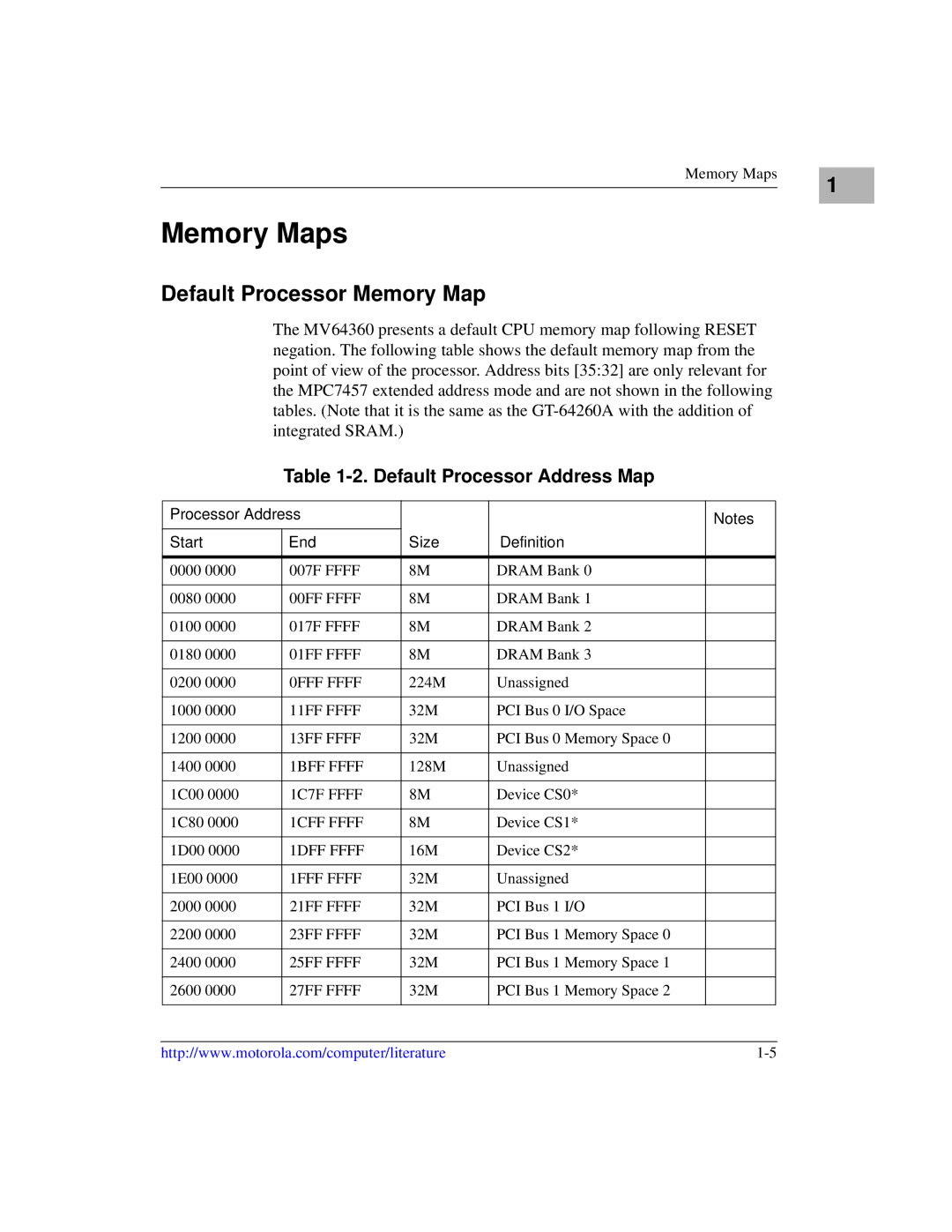
Default Processor Memory Map
The MV64360 presents a default CPU memory map following RESET negation. The following table shows the default memory map from the point of view of the processor. Address bits [35:32] are only relevant for the MPC7457 extended address mode and are not shown in the following tables. (Note that it is the same as the
Table 1-2. Default Processor Address Map
Processor Address |
|
| Notes | |
|
|
|
| |
Start | End | Size | Definition |
|
|
|
|
|
|
0000 0000 | 007F FFFF | 8M | DRAM Bank 0 |
|
|
|
|
|
|
0080 0000 | 00FF FFFF | 8M | DRAM Bank 1 |
|
|
|
|
|
|
0100 0000 | 017F FFFF | 8M | DRAM Bank 2 |
|
|
|
|
|
|
0180 0000 | 01FF FFFF | 8M | DRAM Bank 3 |
|
|
|
|
|
|
0200 0000 | 0FFF FFFF | 224M | Unassigned |
|
|
|
|
|
|
1000 0000 | 11FF FFFF | 32M | PCI Bus 0 I/O Space |
|
|
|
|
|
|
1200 0000 | 13FF FFFF | 32M | PCI Bus 0 Memory Space 0 |
|
|
|
|
|
|
1400 0000 | 1BFF FFFF | 128M | Unassigned |
|
|
|
|
|
|
1C00 0000 | 1C7F FFFF | 8M | Device CS0* |
|
|
|
|
|
|
1C80 0000 | 1CFF FFFF | 8M | Device CS1* |
|
|
|
|
|
|
1D00 0000 | 1DFF FFFF | 16M | Device CS2* |
|
|
|
|
|
|
1E00 0000 | 1FFF FFFF | 32M | Unassigned |
|
|
|
|
|
|
2000 0000 | 21FF FFFF | 32M | PCI Bus 1 I/O |
|
|
|
|
|
|
2200 0000 | 23FF FFFF | 32M | PCI Bus 1 Memory Space 0 |
|
|
|
|
|
|
2400 0000 | 25FF FFFF | 32M | PCI Bus 1 Memory Space 1 |
|
|
|
|
|
|
2600 0000 | 27FF FFFF | 32M | PCI Bus 1 Memory Space 2 |
|
|
|
|
|
|
1
http://www.motorola.com/computer/literature |