|
|
|
| MOTLoad’s PCI Memory Maps |
|
| 1 | |
| Table |
|
| |||||
|
|
|
| |||||
|
|
|
| |||||
|
|
|
|
|
|
|
|
|
| PCI Address |
|
|
|
|
|
|
|
|
|
|
|
|
|
|
|
|
| Start | End | Size | Definition |
|
|
|
|
|
|
|
|
|
|
|
|
|
| F200 0000 | F3FF FFFF | 32M | PCI Bus 1 P2P Memory Space 1 |
|
|
|
|
|
|
|
|
|
|
|
|
|
| F400 0000 | FEFF FFFF | 176M | Unassigned |
|
|
|
|
|
|
|
|
|
|
|
|
|
| FF00 0000 | FF7F FFFF | 8M | Device CS3* |
|
|
|
|
|
|
|
|
|
|
|
|
|
| FC00 0000 | FFFF FFFF | 64M | Boot Flash Bank B |
|
|
|
|
|
|
|
|
|
|
|
|
|
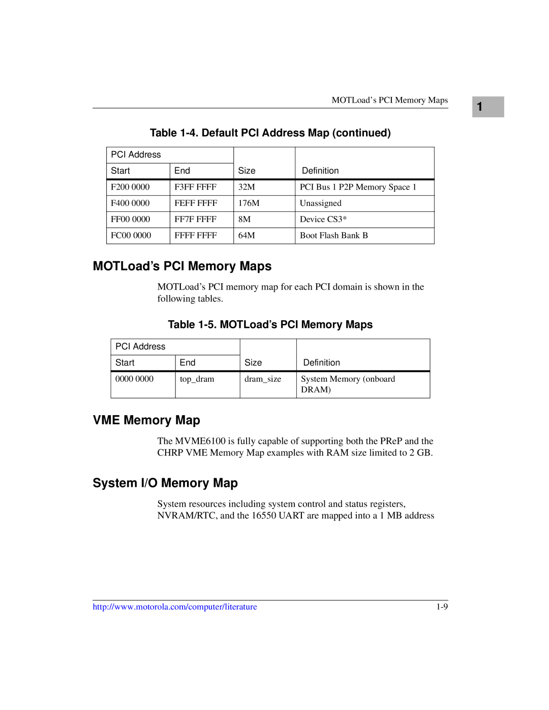
MOTLoad’s PCI Memory Maps
MOTLoad’s PCI memory map for each PCI domain is shown in the following tables.
Table 1-5. MOTLoad’s PCI Memory Maps
PCI Address |
|
|
|
|
|
|
|
Start | End | Size | Definition |
|
|
|
|
0000 0000 | top_dram | dram_size | System Memory (onboard |
|
|
| DRAM) |
|
|
|
|
VME Memory Map
The MVME6100 is fully capable of supporting both the PReP and the
CHRP VME Memory Map examples with RAM size limited to 2 GB.
System I/O Memory Map
System resources including system control and status registers,
NVRAM/RTC, and the 16550 UART are mapped into a 1 MB address
http://www.motorola.com/computer/literature |