AN50 | APPLICATION NOTE |
|
|
Selecting the Inductor
The inductor is one of the most critical components to be selected for a
IPK | = IMIN | VIN – VSW – VD | ||
+ | TON | |||
|
|
|
| |
Where TON is the maximum duty cycle and VD is the forward voltage of diode DS1.
Then the inductor value can be calculated using the relationship:
VIN – VSW – VO | |||
L = | – IMIN | TON | |
|
| ||
Where VSW (RDS,ON x IO) is the
Implementing Short Circuit Protection
Intel currently requires all power supply manufacturers to provide continuous protection against short circuit condi- tions that may damage the CPU. To address this requirement, Raytheon Electronics has implemented a current sense meth- odology to limit the power delivered to the load in the event of overcurrent. The voltage drop created by the output cur- rent across a sense resistor is presented to one terminal of an internal comparator with hysterisis. The other comparator terminal has the threshold voltage, nominally of 120mV. Table 6 states the limits for the comparator threshold of the Switching Regulator.
Table 6. RC5050 Short Circuit Comparator Threshold Voltage
| Short Circuit Comparator |
| Vthreshold (mV) |
Typical | 120 |
|
|
Minimum | 100 |
|
|
Maximum | 140 |
|
|
When designing the external current sense circuitry, pay careful attention to the output limitations during normal operation and during a fault condition. If the short circuit protection threshold current is set too low, the
The following is the design equation used to set the short cir- cuit threshold limit:
RSENSE | Vth | , where: ISC = Output short circuit current | |
= | |||
| ISC |
|
|
ISC ≥ Iinductor | = ILoad, max + | (Ipk – Imin ) | |
Where Ipk and Imin are peak ripple current and Iload, max = maximum output load current.
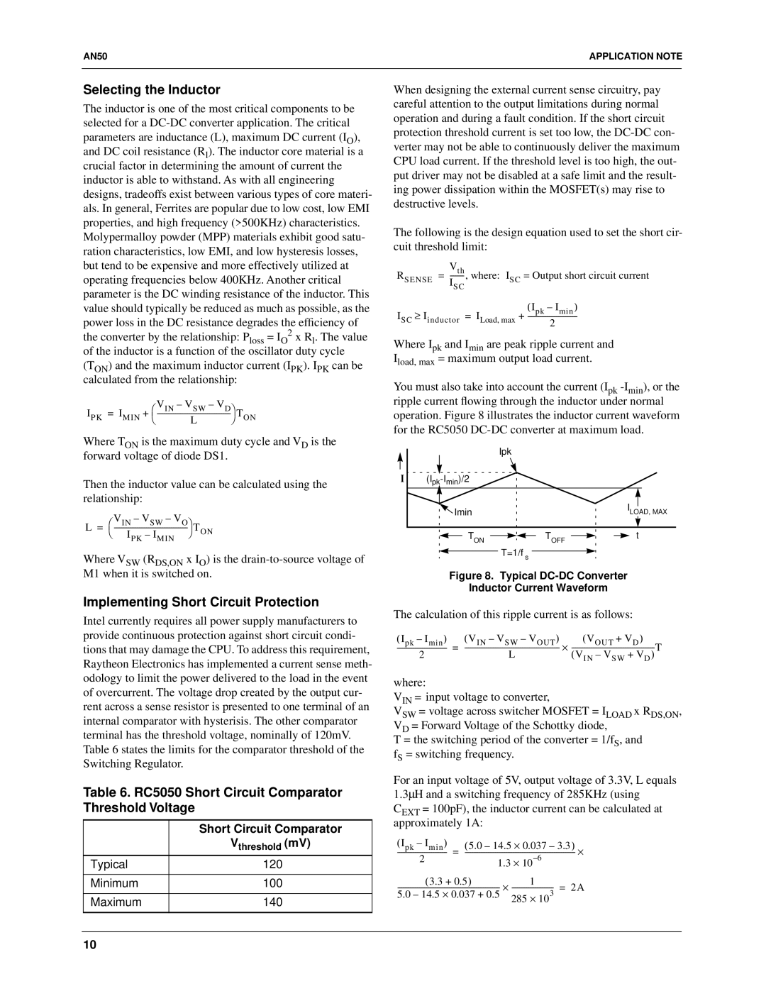
You must also take into account the current (Ipk
operation. Figure 8 illustrates the inductor current waveform for the RC5050
|
| Ipk |
|
I |
|
| |
| Imin |
| ILOAD, MAX |
| TON | TOFF | t |
|
| T=1/f s |
|
Figure 8. Typical DC-DC Converter
Inductor Current Waveform
The calculation of this ripple current is as follows:
(Ipk | – Imin ) | (VIN | – VSW | – VOUT ) | × | (VOUT | + VD ) | T |
- = | L |
| ||||||
| 2 |
|
|
| ||||
where:
VIN = input voltage to converter,
VSW = voltage across switcher MOSFET = ILOAD x RDS,ON, VD = Forward Voltage of the Schottky diode,
T = the switching period of the converter = 1/fS, and fS = switching frequency.
For an input voltage of 5V, output voltage of 3.3V, L equals 1.3∝H and a switching frequency of 285KHz (using CEXT = 100pF), the inductor current can be calculated at approximately 1A:
(Ipk | – Imin ) | (5.0 – 14.5 × 0.037 – 3.3) | × | |||
- = | 1.3 × | - | ||||
| 2 |
|
|
| ||
| (3.3 + 0.5) |
| 3 = 2A | |||
285 × 10 | ||||||
|
|
|
|
|
| |
10