AN50 | APPLICATION NOTE |
|
|
Two MOSFETs in parallel.
We recommend two MOSFETs used in parallel instead of one single MOSFET. The following significant advantages are realized using two MOSFETs in parallel:
•Significant reduction of Power dissipation. Maximum current of 14A with one MOSFET:
PMOSFET = (I2 RDS,ON)(Duty Cycle) =
With two MOSFETs in parallel:
PMOSFET = (I2 RDS,ON)(Duty Cycle) =
*Note: RDS,ON increases with temperature. Assume RDS,ON = 25mΩ at 25°C. RDS,ON can easily increase to 50mΩ at high temperature when using a single MOSFET. When using two MOSFETs in parallel, the
temperature effects should not cause the RDS,ON to rise above the listed maximum value of 37mΩ.
•Less heat sink required.
With power dissipation down to around one watt and with MOSFETs mounted flat on the motherboard, considerable less heat sink is required. The
• Higher current capability.
With thermal management under control, this
MOSFET Gate Bias
MOSFET can be biased by one of two methods: Charge Pump and 12V Gate Bias.
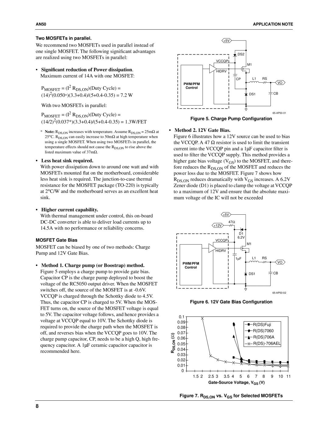
•Method 1. Charge pump (or Boostrap) method. Figure 5 employs a charge pump to provide gate bias. Capacitor CP is the charge pump deployed to boost the voltage of the RC5050 output driver. When the MOSFET switches off, the source of the MOSFET is at
charge pump capacitor, CP, needs to be a high Q, high fre- quency capacitor. A 1µF ceramic capacitor capacitor is
recommended here.
+5V |
|
|
DS2 |
|
|
VCCQP | M1 |
|
|
| |
HIDRV |
|
|
CP | L1 | RS |
PWM/PFM |
| VO |
|
| |
Control |
|
|
| DS1 | CB |
|
|
Figure 5. Charge Pump Configuration
• Method 2. 12V Gate Bias.
Figure 6 illustrates how a 12V source can be used to bias the VCCQP. A 47 Ω resistor is used to limit the transient current into the VCCQP pin and a 1µF capacitor filter is used to filter the VCCQP supply. This method provides a higher gate bias voltage (VGS) to the MOSFET, and there-
fore reduces the RDS,ON of the MOSFET and reduces the power loss due to the MOSFET. Figure 7 shows how
RDS,ON reduces dramatically with VGS increases. A 6.2V Zener diode (D1) is placed to clamp the voltage at VCCQP to a maximum of 12V and ensure that the absolute maxi- mum voltage of the IC will not be exceeded
+5V |
|
|
47Ω |
|
|
+12V |
|
|
D1 |
|
|
6.2V |
|
|
VCCQP | M1 |
|
|
| |
HIDRV |
|
|
1µF | L1 | RS |
PWM/PFM |
| VO |
|
| |
Control |
|
|
| DS1 | CB |
|
|
Figure 6. 12V Gate Bias Configuration
| 0.1 |
|
|
|
|
|
|
|
|
|
|
| 0.09 |
|
|
|
|
| R(DS)Fuji |
|
| ||
| 0.08 |
|
|
|
|
|
|
| |||
|
|
|
|
|
| R(DS)7060 |
|
| |||
) | 0.07 |
|
|
|
|
|
|
| |||
|
|
|
|
|
|
|
|
|
| ||
(Ω | 0.06 |
|
|
|
|
| R(DS)706A |
|
| ||
DS,ON | 0.05 |
|
|
|
|
|
| ||||
0.04 |
|
|
|
|
|
|
|
|
|
| |
R |
|
|
|
|
|
|
|
|
|
| |
0.03 |
|
|
|
|
|
|
|
|
|
| |
|
|
|
|
|
|
|
|
|
|
| |
| 0.02 |
|
|
|
|
|
|
|
|
|
|
| 0.01 |
|
|
|
|
|
|
|
|
|
|
| 0 |
|
|
|
|
|
|
|
|
|
|
| 1.5 2 | 2.5 3 | 3.5 | 4 | 5 | 6 | 7 | 8 | 9 | 10 | 11 |
Figure 7. RDS,ON vs. VGS for Selected MOSFETs
8