AN50APPLICATION NOTE
Table 11. Bill of Materials for a 13A Pentium Pro Klamath Application (continued)
Quantity | Reference | Manufacturer Part | Description | Requirements and |
|
| Order # |
| Comments |
|
|
|
|
|
1 | L1 | Pulse Engineering | 1.3µH inductor |
|
|
|
|
| |
|
|
|
|
|
1 | L2* | Pulse Engineering | 2.5µH inductor | |
|
|
| reduce ripple on 5v line | |
|
|
|
|
|
International Rectifier | RDS,ON < 18mΩ | |||
(note 2) |
| IRF7413 | Enhancement Mode MOSFET | VGS = 4.5V, ID = 5A |
1 | Rsense | Coppel | 6 mΩ, 1W |
|
|
| CuNi Wire resistor |
|
|
|
|
|
|
|
1 | R5 | Panasonic | 47Ω 5% resistors |
|
|
|
|
|
|
|
|
|
|
|
1 | R6 | Panasonic | 10KΩ 5% resistor |
|
|
|
|
|
|
|
|
|
|
|
| U1 | Raytheon | Programmable |
|
|
| RC5050M or RC5051M | converter |
|
|
|
|
|
|
Refer to Appendix A for Directory of component suppliers.
Notes:
1.When used in synchronous mode, a 1A schottky diode such as the 1N5817 should be substituted for the MBR2015CT.
2.A target RDS,ON value of 10mΩ should be used for each output driver switch. Refer to Table 3 for alternative MOSFETs.
PCB Layout Guidelines and Considerations
PCB Layout Guidelines
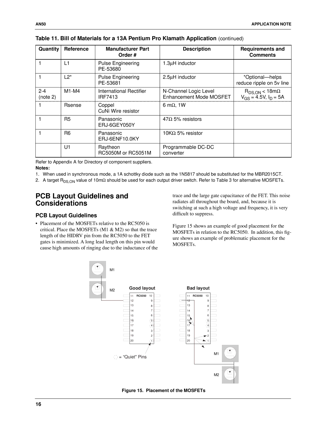
•Placement of the MOSFETs relative to the RC5050 is critical. Place the MOSFETs (M1 & M2) so that the trace length of the HIDRV pin from the RC5050 to the FET gates is minimized. A long lead length on this pin would cause high amounts of ringing due to the inductance of the
trace and the large gate capacitance of the FET. This noise radiates all throughout the board, and, because it is switching at such a high voltage and frequency, it is very difficult to suppress.
Figure 15 shows an example of good placement for the MOSFETs in relation to the RC5050. In addition, this fig- ure shows an example of problematic placement for the MOSFETs.
M1
|
|
|
| M2 | Good layout | ||||
|
|
|
| ||||||
|
|
|
| ||||||
|
|
|
| ||||||
|
|
|
| ||||||
|
|
|
|
|
|
|
|
| |
|
|
|
|
|
| 11 | RC5050 | 10 |
|
|
|
|
|
|
|
| |||
|
|
|
|
|
| 12 |
| 9 |
|
|
|
|
|
|
| 13 |
| 8 |
|
|
|
|
|
|
|
|
| ||
|
|
|
|
|
| 14 |
| 7 |
|
|
|
|
|
|
|
|
| ||
|
|
|
|
|
| 15 |
| 6 |
|
|
|
|
|
|
|
|
| ||
|
|
|
|
|
| 16 |
| 5 |
|
|
|
|
|
|
|
|
| ||
|
|
|
|
|
| 17 |
| 4 |
|
|
|
|
|
|
|
|
| ||
|
|
|
|
|
| 18 |
| 3 |
|
|
|
|
|
|
|
|
| ||
|
|
|
|
|
|
|
| ||
|
|
|
|
|
| 19 |
| 2 |
|
|
|
|
|
|
|
|
| ||
|
|
|
|
|
| 20 |
| 1 |
|
|
|
|
|
|
|
|
| ||
|
|
|
|
|
|
|
| ||
|
|
|
|
|
|
|
|
|
|
![]() = “Quiet" Pins
= “Quiet" Pins
Bad layout
11 RC5050 10
12 | 9 |
13 | 8 |
14 | 7 |
15 | 6 |
16 | 5 |
17 | 4 |
18 | 3 |
19 | 2 |
20 | 1 |
M1
M2
Figure 15. Placement of the MOSFETs
16