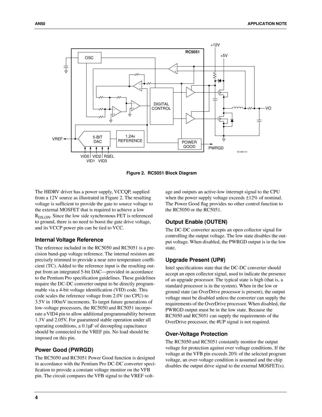
The HIDRV driver has a power supply, VCCQP, supplied from a 12V source as illustrated in Figure 2. The resulting voltage is sufficient to provide the gate to source voltage to the external MOSFET that is required to achieve a low
RDS,ON. Since the low side synchronous FET is referenced to ground, there is no need to boost the gate drive voltage,
and its VCCP power pin can be tied to VCC.
Internal Voltage Reference
The reference included in the RC5050 and RC5051 is a pre- cision band-gap voltage reference. The internal resistors are precisely trimmed to provide a near zero temperature coeffi- cient (TC). Added to the reference input is the resulting out- put from an integrated 5-bit DAC—provided in accordance to the Pentium Pro specification guidelines. These guidelines require the DC-DC converter output to be directly program- mable via a 4-bit voltage identification (VID) code. This code scales the reference voltage from 2.0V (no CPU) to 3.5V in 100mV increments. To target future generations of low-voltage processors, the RC5050 and RC5051 incorpo- rate a VID4 pin to allow additional programmability between 1.3V and 2.05V. For guaranteed stable operation under all operating conditions, a 0.1∝F of decoupling capacitance should be connected to the VREF pin. No load should be imposed on this pin.
Power Good (PWRGD)
The RC5050 and RC5051 Power Good function is designed in accordance with the Pentium Pro DC-DC converter speci- fication to provide a constant voltage monitor on the VFB pin. The circuit compares the VFB signal to the VREF volt-
age and outputs an active-low interrupt signal to the CPU when the power supply voltage exceeds ±12% of nominal. The Power Good flag provides no other control function to the RC5050 or the RC5051.
Output Enable (OUTEN)
The DC-DC converter accepts an open collector signal for controlling the output voltage. The low state disables the out- put voltage. When disabled, the PWRGD output is in the low state.
Upgrade Present (UP#)
Intel specifications state that the DC-DC converter should accept an open collector signal, used to indicate the presence of an upgrade processor. The typical state is high (that is, a standard processor is in the system). When in the low or ground state (an OverDrive processor is present), the output voltage must be disabled unless the converter can supply the requirements of the OverDrive processor. When disabled, the PWRGD output must be in the low state. Because the RC5050 and RC5051 can supply the requirements of the OverDrive processor, the #UP signal is not required.
Over-Voltage Protection
The RC5050 and RC5051 constantly monitor the output voltage for protection against over voltage conditions. If the voltage at the VFB pin exceeds 20% of the selected program voltage, an over-voltage condition is assumed and the chip disables the output drive signal to the external MOSFET(s).