APPLICATION NOTE | AN50 |
|
|
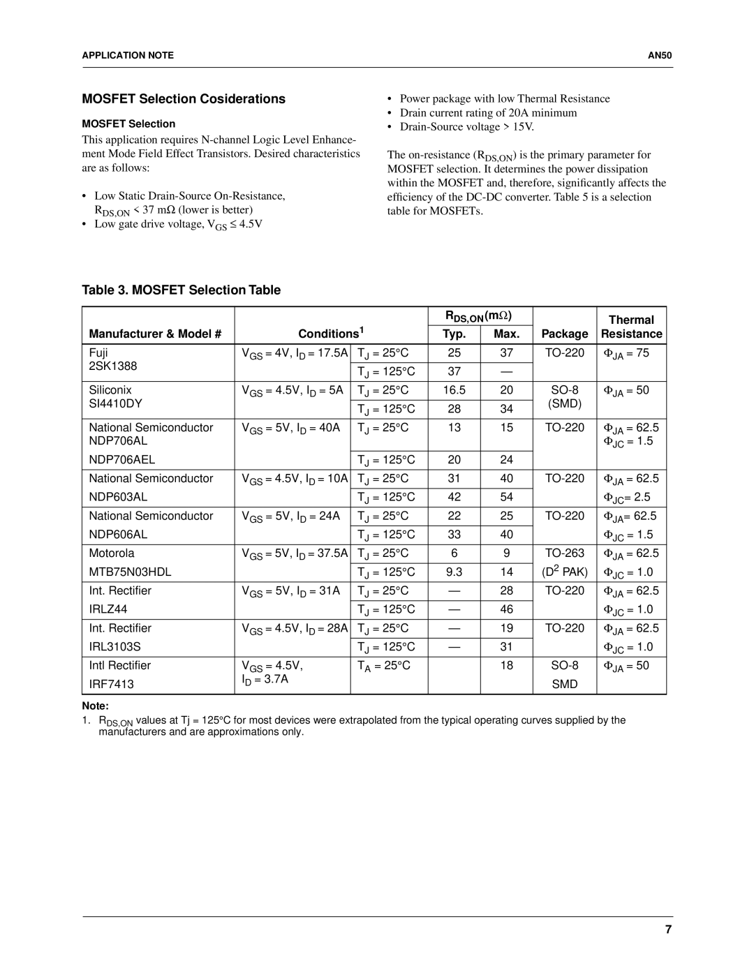
MOSFET Selection Cosiderations
MOSFET Selection
This application requires
•Low Static
•Low gate drive voltage, VGS ≤ 4.5V
•Power package with low Thermal Resistance
•Drain current rating of 20A minimum
•
The
within the MOSFET and, therefore, significantly affects the efficiency of the
Table 3. MOSFET Selection Table
| Conditions1 | RDS,ON(mΩ) |
| Thermal | ||||
Manufacturer & Model # | Typ. | Max. | Package | Resistance | ||||
Fuji | VGS = 4V, ID = 17.5A | TJ = 25°C | 25 | 37 | ΦJA = 75 | |||
2SK1388 |
|
|
|
|
|
|
|
|
| TJ = 125°C | 37 | — |
|
|
|
| |
|
|
|
|
|
| |||
Siliconix | VGS = 4.5V, ID = 5A | TJ = 25°C | 16.5 | 20 | ΦJA = 50 | |||
SI4410DY |
|
|
|
| (SMD) |
|
|
|
| TJ = 125°C | 28 | 34 |
|
|
| ||
|
|
|
|
|
| |||
National Semiconductor | VGS = 5V, ID = 40A | TJ = 25°C | 13 | 15 | ΦJA = 62.5 | |||
NDP706AL |
|
|
|
|
| ΦJC = 1.5 | ||
NDP706AEL |
| TJ = 125°C | 20 | 24 |
|
|
|
|
National Semiconductor | VGS = 4.5V, ID = 10A | TJ = 25°C | 31 | 40 | ΦJA = 62.5 | |||
NDP603AL |
| TJ = 125°C | 42 | 54 |
| ΦJC= 2.5 | ||
National Semiconductor | VGS = 5V, ID = 24A | TJ = 25°C | 22 | 25 | ΦJA= 62.5 | |||
NDP606AL |
| TJ = 125°C | 33 | 40 |
| ΦJC = 1.5 | ||
Motorola | VGS = 5V, ID = 37.5A | TJ = 25°C | 6 | 9 | ΦJA = 62.5 | |||
MTB75N03HDL |
| T = 125°C | 9.3 | 14 | (D2 PAK) | Φ | JC | = 1.0 |
|
| J |
|
|
|
|
| |
Int. Rectifier | VGS = 5V, ID = 31A | TJ = 25°C | — | 28 | ΦJA = 62.5 | |||
IRLZ44 |
| TJ = 125°C | — | 46 |
| ΦJC = 1.0 | ||
Int. Rectifier | VGS = 4.5V, ID = 28A | TJ = 25°C | — | 19 | ΦJA = 62.5 | |||
IRL3103S |
| TJ = 125°C | — | 31 |
| ΦJC = 1.0 | ||
Intl Rectifier | VGS = 4.5V, | TA = 25°C |
| 18 | ΦJA = 50 | |||
IRF7413 | ID = 3.7A |
|
|
| SMD |
|
|
|
Note:
1.RDS,ON values at Tj = 125°C for most devices were extrapolated from the typical operating curves supplied by the manufacturers and are approximations only.
7