APPLICATION NOTE | AN50 |
|
|
Short Circuit Protection
A current sense methodology is implemented to disable the output drive signal to the MOSFET(s) when an
The
In general, a lower operating frequency decreases the peak ripple current flowing in the output inductor, thus allowing the use of a smaller inductor value. Unfortunately, operation at lower frequencies increases the amount of energy storage that must be provided by the bulk output capacitors during load transients due to slower loop response of the controller.
In addition, the efficiency losses due to switching of the MOSFETs increase as the operating frequency is increased. Thus, efficiency is optimized at lower operating frequencies. An operating frequency of 300 kHz was chosen to optimize efficiency while maintaining excellent regulation and tran- sient performance under all operating conditions.
Oscillator
The RC5050 and RC5051 oscillator section uses a fixed cur- rent capacitor charging configuration. An external capacitor (CEXT) is used to preset the oscillator frequency between 200KHz and 1MHz. This scheme allows maximum flexibil- ity in setting the switching frequency and in choosing exter- nal components.
Design Considerations and Component Selection
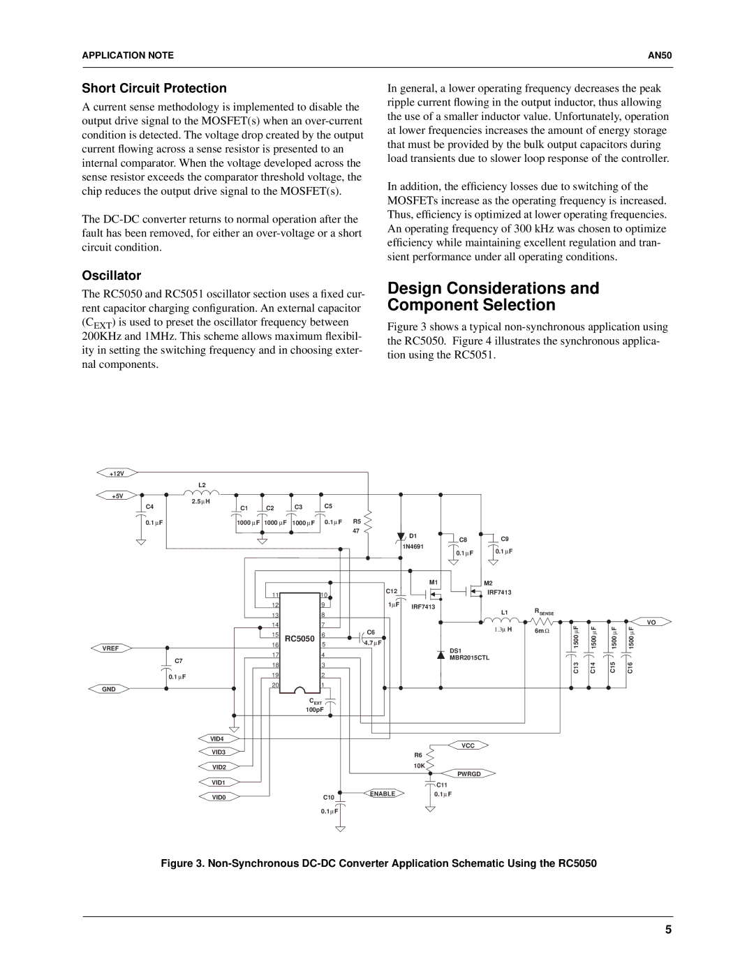
Figure 3 shows a typical non-synchronous application using the RC5050. Figure 4 illustrates the synchronous applica- tion using the RC5051.
+12V |
|
|
|
|
|
|
|
|
|
|
|
|
|
|
L2 |
|
|
|
|
|
|
|
|
|
|
|
|
| |
+5V | μH |
|
|
|
|
|
|
|
|
|
|
|
|
|
2.5 |
|
|
| C5 |
|
|
|
|
|
|
|
|
| |
C4 | C1 | C2 |
| C3 |
|
|
|
|
|
|
|
|
| |
0.1 μF | 1000 μ F | 1000 μF | 1000 μ F | 0.1 μ F | R5 |
|
|
|
|
|
|
|
| |
|
|
|
|
|
| 47 | D1 |
|
|
|
|
|
|
|
|
|
|
|
|
|
| C8 | C9 |
|
|
|
|
| |
|
|
|
|
|
|
| 1N4691 |
|
|
|
|
| ||
|
|
|
|
|
|
| 0.1 μ F | 0.1 μF |
|
|
|
|
| |
|
|
|
|
|
|
|
|
|
|
|
|
| ||
|
|
|
|
|
|
|
| M1 | M2 |
|
|
|
|
|
|
| 11 |
|
| 10 | C12 |
|
| IRF7413 |
|
|
|
|
|
|
|
|
|
|
|
|
|
|
|
|
|
| ||
|
| 12 |
|
| 9 | 1μF | IRF7413 |
| R SENSE |
|
|
|
| |
|
|
|
|
|
|
| L1 |
|
|
|
| |||
|
| 13 |
|
| 8 |
|
|
|
|
|
|
| ||
|
| 14 |
|
| 7 |
|
|
| 1.3μ H |
| μF | μF |
| VO |
|
|
|
|
|
|
| 6m Ω | μF | μF | |||||
|
| 15 | RC5050 | 6 | C6 |
|
| |||||||
|
| 4.7 μF |
|
|
|
| 1500 | 1500 | 1500 | 1500 | ||||
VREF |
| 16 |
|
| 5 |
| DS1 |
|
| |||||
| 17 |
|
| 4 |
|
|
|
|
|
|
|
| ||
|
|
|
|
|
|
|
|
|
|
|
| |||
C7 |
|
|
|
|
| MBR2015CTL |
|
|
|
|
| |||
|
|
|
|
|
|
|
| C13 | C14 | C15 | C16 | |||
| 18 |
|
| 3 |
|
|
|
|
| |||||
|
|
|
|
|
|
|
|
| ||||||
0.1 μF |
| 19 |
|
| 2 |
|
|
|
|
|
|
|
|
|
GND |
| 20 |
|
| 1 |
|
|
|
|
|
|
|
|
|
|
|
|
|
|
|
|
|
|
|
|
|
|
| |
|
|
|
| CEXT |
|
|
|
|
|
|
|
|
| |
|
|
|
| 100pF |
|
|
|
|
|
|
|
|
| |
| VID4 |
|
|
|
|
|
| VCC |
|
|
|
|
|
|
| VID3 |
|
|
|
|
|
|
|
|
|
|
|
| |
|
|
|
|
|
| R6 |
|
|
|
|
|
|
| |
|
|
|
|
|
|
|
|
|
|
|
|
|
| |
| VID2 |
|
|
|
|
| 10K | PWRGD |
|
|
|
|
|
|
|
|
|
|
|
|
|
|
|
|
|
|
|
| |
| VID1 |
|
|
|
|
|
| C11 |
|
|
|
|
|
|
|
|
|
|
|
|
|
|
|
|
|
|
|
| |
| VID0 |
|
|
| C10 | ENABLE |
| 0.1 μ F |
|
|
|
|
|
|
|
|
|
|
|
|
|
|
|
|
|
|
| ||
|
|
|
|
| 0.1 μ F |
|
|
|
|
|
|
|
|
|
Figure 3. Non-Synchronous DC-DC Converter Application Schematic Using the RC5050
5
