APPLICATION NOTE | AN50 |
|
|
In general, all of the noisy switching lines should be kept away from the quiet analog section of the RC5050. That is, traces that connect to pins 12 and 13 (HIDRV and VCCQP) should be kept far away from the traces that con- nect to pins 1 through 5, and pin 16.
•Place the 0.1∝F decoupling capacitors as close to the RC5050 pins as possible. Extra lead length negates their ability to suppress noise.
•Each VCC and GND pin should have its own via to the appropriate plane. This helps to provide isolation between pins.
•Surround the CEXT timing capacitor with a ground trace. Be sure to place a ground or power plane under the capacitor for further noise isolation to provide additional shielding to the oscillator pin 1 from the noise on the PCB. In addition, place this capacitor as close to the RC5050 pin 1 as possible.
•Place the MOSFETs, inductor and Schottky as close together as possible for the same reasons on the first bullet above. Place the input bulk capacitors as close to the
drains of MOSFETs as possible. In addition, placement of a 0.1∝F decoupling capacitor right on the drain of each
MOSFET helps to suppress some of the high frequency switching noise on the input of the
•Place the output bulk capacitors as close to the CPU as possible to optimize their ability to supply instantaneous current to the load in the event of a current transient. Additional space between the output capacitors and the CPU allows the parasitic resistance of the board traces to degrade the
•The traces that run from the RC5050 IFB (pin 4) and VFB (pin 5) pins should be run next to each other and Kelvin connected to the sense resistor. Running these lines together prevents some of the common mode noise that is presented to the RC5050 feedback input. Try, as much as possible, to run the noisy switching signals (HIDRV & VCCQP) on one layer, but use the inner layers for power and ground only. If the top layer is being used to route all of the noisy switching signals, use the bottom layer to route the analog sensing signals VFB and IFB.
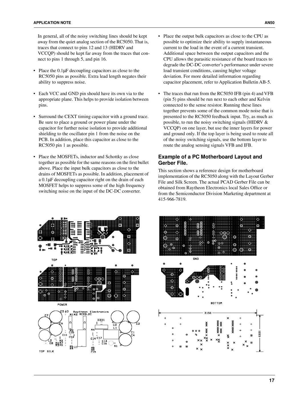
Example of a PC Motherboard Layout and Gerber File.
This section shows a reference design for motherboard implementation of the RC5050 along with the Layout Gerber File and Silk Screen. The actual PCAD Gerber File can be obtained from Raytheon Electronics local Sales Office or from the Semiconductor Division Marketing department at
17
