Chapter 5 Usage
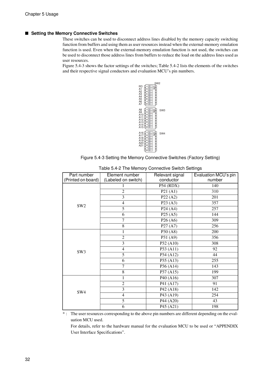
■Setting the Memory Connective Switches
These switches can be used to disconnect address lines disabled by the memory capacity switching function from buffers and using them as user resources instead when the
Figure 5.4-3 shows the factor settings of the switches; Table 5.4-2 lists the elements of the switches and their respective signal conductors and evaluation MCU’s pin numbers.
|
|
|
|
|
| SW2 | ||
RD |
| 1 2 |
|
|
| ON |
|
|
A1 |
|
|
|
|
|
| ||
A2 |
| 3 |
|
|
|
|
|
|
A3 |
| 4 |
|
|
|
|
|
|
A4 |
| 5 |
|
|
|
|
|
|
A5 |
| 6 |
|
|
|
|
|
|
A6 |
| 7 |
|
|
|
|
|
|
A7 |
| 8 |
|
|
|
|
|
|
|
|
|
|
|
|
|
|
|
|
|
|
|
|
|
|
| |
A8 |
| 1 2 |
|
|
| ON |
| SW3 |
A9 |
|
|
|
|
| |||
A10 |
| 3 |
|
|
|
|
|
|
A11 |
| 4 |
|
|
|
|
|
|
A12 |
| 5 |
|
|
|
|
|
|
A13 |
| 6 |
|
|
|
|
|
|
A14 |
| 7 |
|
|
|
|
|
|
A15 |
| 8 |
|
|
|
|
|
|
|
|
|
|
|
|
|
|
|
|
|
|
|
|
|
|
| |
A16 |
| 1 2 |
|
|
| ON |
| SW4 |
A17 |
|
|
|
|
|
| ||
A18 |
| 3 |
|
|
|
|
|
|
A19 |
| 4 |
|
|
|
|
|
|
A20 |
| 5 |
|
|
|
|
|
|
A21 |
| 6 |
|
|
|
|
|
|
|
| 7 |
|
|
|
|
|
|
|
| 8 |
|
|
|
|
|
|
|
|
|
|
|
|
|
|
|
Figure 5.4-3 Setting the Memory Connective Switches (Factory Setting)
Table 5.4-2 The Memory Connective Switch Settings
Part number | Element number | Relevant signal | Evaluation MCU’s pin | |
(Printed on board) | (Labeled on switch) | conductor | number | |
|
|
|
| |
| 1 | P54 (RDX) | 140 | |
|
|
|
| |
| 2 | P21 (A1) | 310 | |
|
|
|
| |
| 3 | P22 (A2) | 201 | |
|
|
|
| |
SW2 | 4 | P23 (A3) | 357 | |
|
|
| ||
5 | P24 (A4) | 257 | ||
| ||||
|
|
|
| |
| 6 | P25 (A5) | 144 | |
|
|
|
| |
| 7 | P26 (A6) | 309 | |
|
|
|
| |
| 8 | P27 (A7) | 256 | |
|
|
|
| |
| 1 | P30 (A8) | 200 | |
|
|
|
| |
| 2 | P31 (A9) | 356 | |
|
|
|
| |
| 3 | P32 (A10) | 308 | |
|
|
|
| |
SW3 | 4 | P33 (A11) | 92 | |
|
|
| ||
5 | P34 (A12) | 44 | ||
| ||||
|
|
|
| |
| 6 | P35 (A13) | 255 | |
|
|
|
| |
| 7 | P36 (A14) | 143 | |
|
|
|
| |
| 8 | P37 (A15) | 199 | |
|
|
|
| |
| 1 | P40 (A16) | 307 | |
|
|
|
| |
| 2 | P41 (A17) | 91 | |
|
|
|
| |
SW4 | 3 | P42 (A18) | 142 | |
|
|
| ||
4 | P43 (A19) | 254 | ||
| ||||
|
|
|
| |
| 5 | P44 (A20) | 43 | |
|
|
|
| |
| 6 | P45 (A21) | 198 |
*: The user resources corresponding to the above pin numbers are different depending on the eval- uation MCU used.
For details, refer to the hardware manual for the evaluation MCU to be used or “APPENDIX User Interface Specifications”.
32