The filtered signals are applied to the limiter amplifier (IC3), and are then mixed with the DTMF signal from the CPU (IC33, pin 43) via the
•IN CASE OF THE AF SIGNALS FROM THE ANTENNA CONNECTOR
The AF signals (received signals) from the antenna connec- tor (RX unit; J1) are applied to the buffer amplifier (IC9), CTCSS detector (IC29) and AF amplifier (IC6). The ampli- fied signals are applied to the D/A converter IC (IC25, pins 8, 9) to adjust a repeater AF level. The adjusted AF signals pass through the RPT AF mute switch (IC14), and are applied to the limiter amplifier (IC3).
•IN CASE OF THE 2/5TONE SIGNALS
The 2/5TONE signals from the CPU (IC33, pin 43) are applied to the mixer amplifier (IC3) via TX signal filter circuit (IC3, pins 8, 10, 12, 14).
•IN CASE OF THE DTMF SIGNALS FROM
DIALER IC
The DTMF from dialer IC (IC47, pin 14) are applied to the mixer amplifier (IC3) via the TX signal filter circuit (IC3, pins 8, 10, 12, 14).
•IN CASE OF THE CTCSS AND DTCS SIGNALS
FROM THE CPU
The CTCSS and DTCS signals from the CPU (IC33, pin 44) are applied to the
3-2-2 MODULATION CIRCUIT (TX UNIT)
The modulation circuit modulates the VCO oscillating signal (RF signal) using the AF audio signals.
The filtered signals from the LOGIC unit are applied to the D/A converter (IC5, pin 4) to adjust AF level. The adjusted signals are applied to the mixer amplifier IC (IC6, pin 1) with the CTCSS/DTCS signals.
The mixed signals are applied to the TX VCO circuit to mod-
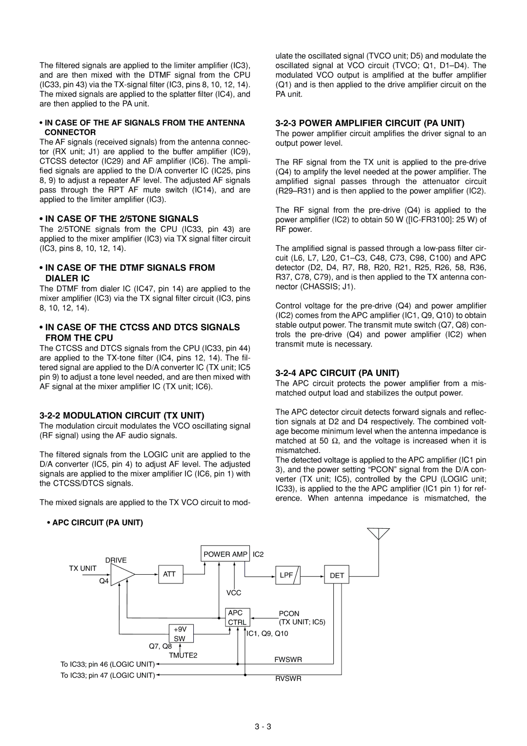
•APC CIRCUIT (PA UNIT)
ulate the oscillated signal (TVCO unit; D5) and modulate the oscillated signal at VCO circuit (TVCO; Q1,
3-2-3 POWER AMPLIFIER CIRCUIT (PA UNIT)
The power amplifier circuit amplifies the driver signal to an output power level.
The RF signal from the TX unit is applied to the
The RF signal from the
The amplified signal is passed through a
Control voltage for the
3-2-4 APC CIRCUIT (PA UNIT)
The APC circuit protects the power amplifier from a mis- matched output load and stabilizes the output power.
The APC detector circuit detects forward signals and reflec- tion signals at D2 and D4 respectively. The combined volt- age become minimum level when the antenna impedance is matched at 50 Ω, and the voltage is increased when it is mismatched.
The detected voltage is applied to the APC amplifier (IC1 pin 3), and the power setting “PCON” signal from the D/A con- verter (TX unit; IC5), controlled by the CPU (LOGIC unit; IC33), is applied to the the APC amplifier (IC1 pin 1) for ref- erence. When antenna impedance is mismatched, the
DRIVE
POWER AMP IC2
TX UNIT
Q4
ATT
LPF
VCC
DET
|
|
|
|
| APC | PCON |
| |
|
|
|
|
| CTRL | (TX UNIT; IC5) |
| |
|
| +9V |
|
| IC1, Q9, Q10 |
| ||
|
| SW |
|
|
| |||
|
|
|
|
|
| |||
Q7, Q8 |
|
|
|
|
|
| ||
|
|
|
|
| ||||
|
| TMUTE2 |
| FWSWR |
| |||
To IC33; pin 46 (LOGIC UNIT) |
|
|
|
|
|
|
| |
|
|
|
|
|
| |||
To IC33; pin 47 (LOGIC UNIT) |
|
|
|
|
|
| ||
|
|
|
| RVSWR |
| |||
|
|
|
|
|
|
|
| |
3 - 3