Intel UPI-L42 specifications Program Memory Bank Switch, UPI-C42 Features, Interrupt Routines

Models: UPI-L42 UPI-C42

1 25
Download 25 pages 38.88 Kb
Page 6
Image 6

UPI-C42/UPI-L42

If ‘‘EN DMA’’ has been executed, P27 becomes the DACK (DMA ACKnowledge) pin. This pin acts as a chip select input for the Data Bus Buffer registers during DMA transfers.

EN DMA

Op Code: 0E5H


1


1

1

0


0

1

0

1


D7


D0

6.When EA is enabled on the UPI, the program counter is placed on Port 1 and the lower four

bits of Port 2 (MSB e P23, LSB e P10). On the UPI this information is multiplexed with PORT DATA (see port timing diagrams at end of this data sheet).

7.The UPI-C42 supports the Quick Pulse Program- ming Algorithm, but can also be programmed with the Intelligent Programming Algorithm. (See the Programming Section.)

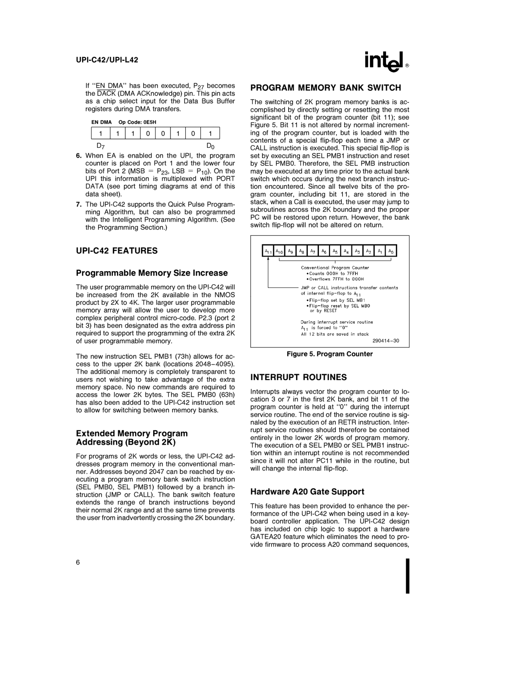
PROGRAM MEMORY BANK SWITCH

The switching of 2K program memory banks is ac- complished by directly setting or resetting the most significant bit of the program counter (bit 11); see Figure 5. Bit 11 is not altered by normal increment- ing of the program counter, but is loaded with the contents of a special flip-flop each time a JMP or CALL instruction is executed. This special flip-flop is set by executing an SEL PMB1 instruction and reset by SEL PMB0. Therefore, the SEL PMB instruction may be executed at any time prior to the actual bank switch which occurs during the next branch instruc- tion encountered. Since all twelve bits of the pro- gram counter, including bit 11, are stored in the stack, when a Call is executed, the user may jump to subroutines across the 2K boundary and the proper PC will be restored upon return. However, the bank switch flip-flop will not be altered on return.

UPI-C42 FEATURES

Programmable Memory Size Increase

The user programmable memory on the UPI-C42 will be increased from the 2K available in the NMOS product by 2X to 4K. The larger user programmable memory array will allow the user to develop more complex peripheral control micro-code. P2.3 (port 2 bit 3) has been designated as the extra address pin required to support the programming of the extra 2K of user programmable memory.

The new instruction SEL PMB1 (73h) allows for ac- cess to the upper 2K bank (locations 2048 – 4095). The additional memory is completely transparent to users not wishing to take advantage of the extra memory space. No new commands are required to access the lower 2K bytes. The SEL PMB0 (63h) has also been added to the UPI-C42 instruction set to allow for switching between memory banks.

Extended Memory Program

Addressing (Beyond 2K)

For programs of 2K words or less, the UPI-C42 ad- dresses program memory in the conventional man- ner. Addresses beyond 2047 can be reached by ex- ecuting a program memory bank switch instruction (SEL PMB0, SEL PMB1) followed by a branch in- struction (JMP or CALL). The bank switch feature extends the range of branch instructions beyond their normal 2K range and at the same time prevents the user from inadvertently crossing the 2K boundary.

290414 – 30

Figure 5. Program Counter

INTERRUPT ROUTINES

Interrupts always vector the program counter to lo- cation 3 or 7 in the first 2K bank, and bit 11 of the program counter is held at ‘‘0’’ during the interrupt service routine. The end of the service routine is sig- naled by the execution of an RETR instruction. Inter- rupt service routines should therefore be contained entirely in the lower 2K words of program memory. The execution of a SEL PMB0 or SEL PMB1 instruc- tion within an interrupt routine is not recommended since it will not alter PC11 while in the routine, but will change the internal flip-flop.

Hardware A20 Gate Support

This feature has been provided to enhance the per- formance of the UPI-C42 when being used in a key- board controller application. The UPI-C42 design has included on chip logic to support a hardware GATEA20 feature which eliminates the need to pro- vide firmware to process A20 command sequences,

6

Page 6
Image 6
Intel UPI-L42 specifications Program Memory Bank Switch, UPI-C42 Features, Interrupt Routines