TK-260G/270G
CIRCUIT DESCRIPTION
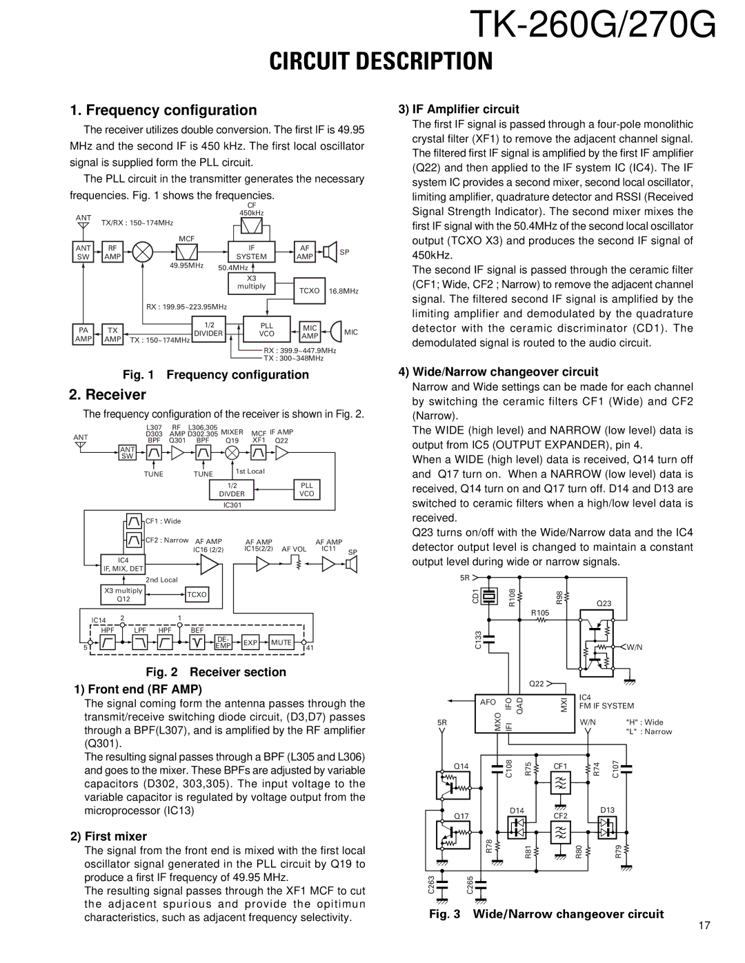
1. Frequency configuration
The receiver utilizes double conversion. The first IF is 49.95 MHz and the second IF is 450 kHz. The first local oscillator signal is supplied form the PLL circuit.
The PLL circuit in the transmitter generates the necessary frequencies. Fig. 1 shows the frequencies.
3) IF Amplifier circuit |
The first IF signal is passed through a |
crystal filter (XF1) to remove the adjacent channel signal. |
The filtered first IF signal is amplified by the first IF amplifier |
(Q22) and then applied to the lF system IC (IC4). The IF |
system IC provides a second mixer, second local oscillator, |
limiting amplifier, quadrature detector and RSSI (Received |
|
|
|
|
|
|
|
|
|
| CF |
|
|
| ||
ANT |
|
|
|
|
|
|
|
| 450kHz |
|
|
| |||
TX/RX : 150~174MHz |
|
|
|
|
|
|
|
|
| ||||||
|
|
|
|
|
|
|
|
|
| ||||||
|
|
|
|
| MCF |
|
|
|
|
|
|
|
|
| |
|
|
|
|
|
|
|
|
|
|
|
|
|
| ||
ANT | RF |
|
|
|
|
|
|
|
| IF |
|
|
| ||
SW | AMP |
|
| 49.95MHz |
|
| SYSTEM |
|
|
| |||||
|
|
|
| 50.4MHz |
|
|
|
|
| ||||||
|
|
|
|
|
|
|
| ||||||||
|
|
|
|
|
|
|
|
|
|
| |||||
|
|
|
|
|
|
|
|
|
| X3 |
|
|
| ||
|
|
|
|
|
|
|
|
|
|
|
|
| |||
|
|
|
|
|
|
|
|
| multiply |
|
|
| |||
|
|
|
|
|
|
|
|
|
|
|
| ||||
|
|
| RX : 199.95~223.95MHz |
|
|
| |||||||||
|
|
|
|
|
| ||||||||||
|
|
|
|
|
| ||||||||||
AF ![]() SP AMP
SP AMP
TCXO 16.8MHz
Signal Strength Indicator). The second mixer mixes the |
first IF signal with the 50.4MHz of the second local oscillator |
output (TCXO X3) and produces the second IF signal of |
450kHz. |
The second IF signal is passed through the ceramic filter |
(CF1; Wide, CF2 ; Narrow) to remove the adjacent channel |
signal. The filtered second IF signal is amplified by the |
limiting amplifier and demodulated by the quadrature |
PA |
| TX |
|
|
| 1/2 |
|
|
|
| PLL |
| MIC |
|
| MIC | |
|
|
|
|
|
|
|
| ||||||||||
AMP |
|
|
|
| DIVIDER |
|
|
| VCO |
| AMP | ||||||
| AMP | TX : 150~174MHz |
|
|
|
|
|
|
|
|
|
| |||||
|
|
|
|
|
|
|
|
|
|
|
| RX : 399.9~447.9MHz |
| ||||
|
|
|
|
|
|
|
|
|
|
|
|
| |||||
|
|
|
|
|
|
|
|
|
|
|
| TX : 300~348MHz |
| ||||
|
|
|
|
|
|
|
|
|
|
|
|
| |||||
detector with the ceramic discriminator (CD1). The |
demodulated signal is routed to the audio circuit. |
Fig. 1 Frequency configuration
2. Receiver
The frequency configuration of the receiver is shown in Fig. 2.
| L307 | RF | L306,305 | MIXER | MCF IF AMP | |
ANT | D303 | AMP D302.305 | ||||
BPF | Q301 | BPF | Q19 | XF1 Q22 | ||
| ||||||
| ANT |
|
|
|
|
|
| |
| SW |
|
|
|
|
|
|
|
|
| TUNE | TUNE | 1st Local |
|
|
| |
|
|
|
|
|
| |||
|
|
|
|
| 1/2 | PLL |
|
|
|
|
|
| DIVDER | VCO |
|
| |
|
|
|
| IC301 |
|
|
| |
|
| CF1 : Wide |
|
|
|
|
| |
|
| CF2 : Narrow | AF AMP | AF AMP |
| AF AMP |
| |
|
|
|
| IC16 (2/2) | IC15(2/2) | AF VOL | IC11 | SP |
| IC4 |
|
|
|
|
|
| |
|
|
|
|
|
|
|
| |
IF, MIX, DET |
|
|
|
|
|
| ||
|
| 2nd Local |
|
|
|
|
| |
X3 multiply | TCXO |
|
|
|
| |||
| Q12 |
|
|
|
|
| ||
|
|
|
|
|
|
|
| |
IC14 | 2 |
| 1 |
|
|
|
|
|
|
|
|
|
|
|
|
| |
HPF |
| LPF | HPF | BEF |
|
|
|
|
4)Wide/Narrow changeover circuit
Narrow and Wide settings can be made for each channel by switching the ceramic filters CF1 (Wide) and CF2 (Narrow).
The WIDE (high level) and NARROW (low level) data is output from IC5 (OUTPUT EXPANDER), pin 4.
When a WIDE (high level) data is received, Q14 turn off and Q17 turn on. When a NARROW (low level) data is received, Q14 turn on and Q17 turn off. D14 and D13 are switched to ceramic filters when a high/low level data is received.
Q23 turns on/off with the Wide/Narrow data and the IC4 detector output level is changed to maintain a constant output level during wide or narrow signals.
5R ![]()
CD1 | R108 | R98 | Q23 |
|
| R105 |
|
| DE- | EXP | MUTE | |
5 | EMP | |||
| 41 |
Fig. 2 Receiver section 1) Front end (RF AMP)
The signal coming form the antenna passes through the transmit/receive switching diode circuit, (D3,D7) passes through a BPF(L307), and is amplified by the RF amplifier
5R
| C133 |
|
|
|
| Q22 | ||
|
|
|
|
|
| |||
|
|
|
|
|
| |||
|
|
|
|
|
|
|
| |
|
|
|
|
|
|
|
| |
|
|
|
|
|
|
|
|
|
|
|
|
|
|
| MXO IFIIFO QAD | MXI | |
|
| AFO |
| |||||
W/N
IC4
FM IF SYSTEM
W/N "H" : Wide
"L" : Narrow
(Q301).
The resulting signal passes through a BPF (L305 and L306) and goes to the mixer. These BPFs are adjusted by variable capacitors (D302, 303,305). The input voltage to the variable capacitor is regulated by voltage output from the microprocessor (IC13)
2) First mixer |
The signal from the front end is mixed with the first local |
oscillator signal generated in the PLL circuit by Q19 to |
produce a first IF frequency of 49.95 MHz. |
The resulting signal passes through the XF1 MCF to cut |
the adjacent spurious and provide the opitimun |
Q14 | C108 | R75 |
|
| |
Q17 | D14 |
|
|
| |
| R78 | R81 |
C263 | C265 |
CF1
CF2
R74 | C107 |
| D13 |
R80 | R79 |
characteristics, such as adjacent frequency selectivity. |
Fig. 3 Wide/Narrow changeover circuit
17