TK-260G/270G
CIRCUIT DESCRIPTION/SEMICONDUCTOR DATA
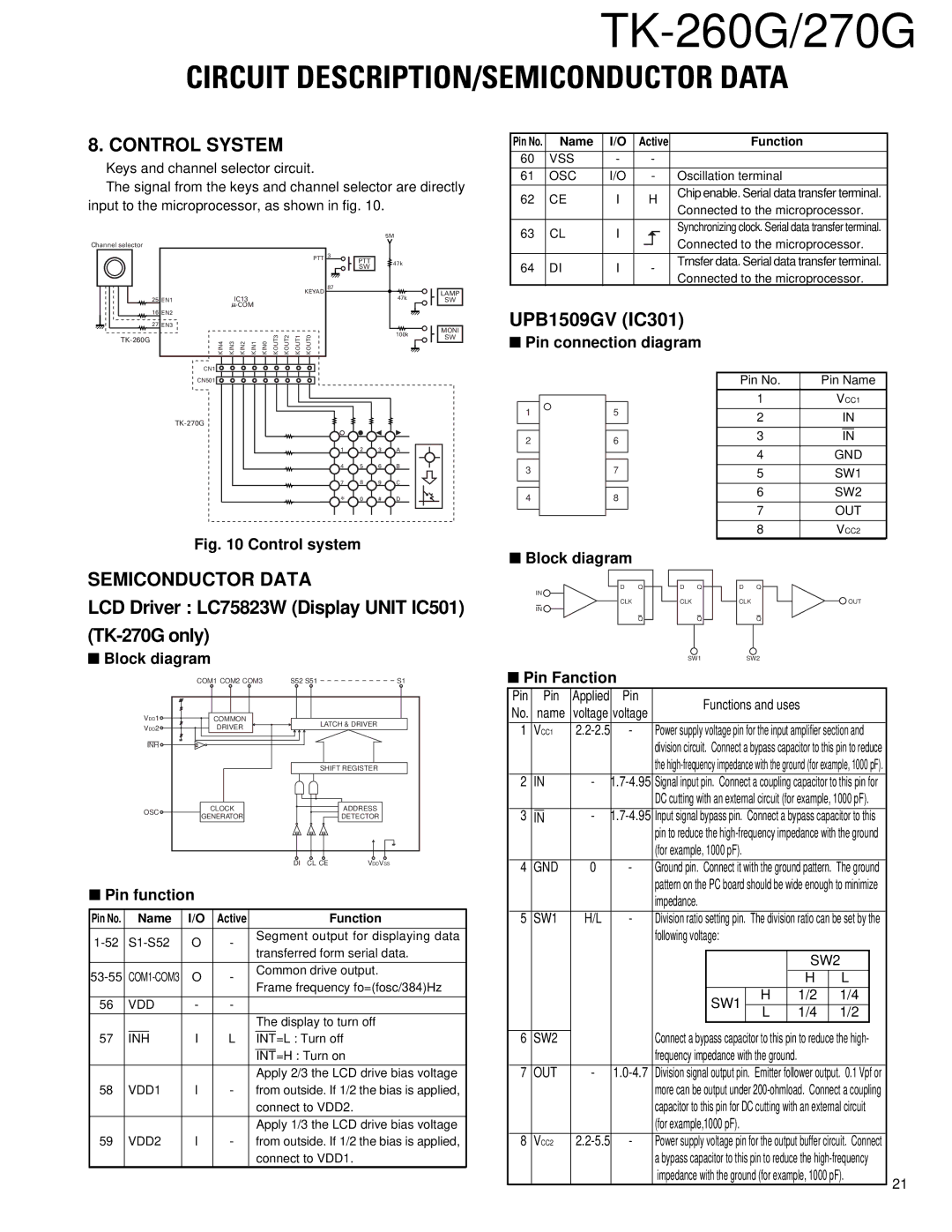
8. CONTROL SYSTEM
Keys and channel selector circuit.
The signal from the keys and channel selector are directly input to the microprocessor, as shown in fig. 10.
Pin No. | Name | I/O | Active | Function | |||
60 | VSS | - | - |
|
| ||
|
|
|
|
|
|
| |
61 | OSC | I/O | - |
| Oscillation terminal | ||
62 | CE | I | H | Chip enable. Serial data transfer terminal. | |||
Connected to the microprocessor. | |||||||
|
|
|
|
|
| ||
|
|
|
|
|
|
| |
63 | CL | I |
|
|
| Synchronizing clock. Serial data transfer terminal. | |
Channel selector
25 EN1
16 EN2
27 EN3
PTT 3
KEYAD 87
IC13
KIN4 | KIN3 | KIN2 | KIN1 | KIN0 | KOUT3 | KOUT2 | KOUT1 | KOUT0 |
CN1 ![]()
![]()
PTT SW
5M
![]() 47k
47k
47k
100k
LAMP
SW
MONI
SW
|
|
|
| Connected to the microprocessor. | |
|
|
|
| ||
64 DI | I | - | Trnsfer data. Serial data transfer terminal. | ||
Connected to the microprocessor. | |||||
|
|
|
| ||
UPB1509GV (IC301)
■Pin connection diagram
CN501 ![]()
![]()
1
5
Pin No. | Pin Name |
1 | VCC1 |
|
|
2 | IN |
|
|
| |
1 | 2 | 3 | A |
4 | 5 | 6 | B |
7 | 8 | 9 | C |
∗ | 0 | # | D |
Fig. 10 Control system
2
3
4
6
7
8
3 | IN |
4 | GND |
|
|
5 | SW1 |
|
|
6 | SW2 |
|
|
7 | OUT |
|
|
8 | VCC2 |
SEMICONDUCTOR DATA
LCD Driver : LC75823W (Display UNIT IC501)
(TK-270G only)
■Block diagram
| COM1 COM2 COM3 | S52 S51 | S1 | |
VDD1 | COMMON |
| LATCH & DRIVER | |
VDD2 | DRIVER |
| ||
|
|
| ||
INH |
|
|
|
|
|
|
| SHIFT REGISTER | |
OSC | CLOCK |
|
| ADDRESS |
GENERATOR |
|
| DETECTOR | |
|
|
| ||
|
| DI | CL CE | VDDVSS |
■Pin function
Pin No. |
| Name | I/O | Active |
|
| Function | |
|
|
|
|
|
|
|
|
|
O | - |
| Segment output for displaying data | |||||
| transferred form serial data. | |||||||
|
|
|
|
|
|
| ||
|
|
|
|
|
|
|
|
|
O | - |
| Common drive output. | |||||
| Frame frequency fo=(fosc/384)Hz | |||||||
|
|
|
|
|
|
| ||
|
|
|
|
|
|
|
|
|
56 | VDD | - | - |
|
|
| ||
|
|
|
|
|
|
|
|
|
|
|
|
|
|
|
| The display to turn off | |
57 |
|
|
| I | L |
|
|
|
| INH |
|
| INT=L : Turn off | ||||
|
|
|
|
|
|
|
|
|
|
|
|
|
|
|
| INT=H : Turn on | |
|
|
|
|
|
|
| Apply 2/3 the LCD drive bias voltage | |
58 | VDD1 | I | - |
| from outside. If 1/2 the bias is applied, | |||
|
|
|
|
|
|
| connect to VDD2. | |
|
|
|
|
|
|
|
|
|
|
|
|
|
|
|
| Apply 1/3 the LCD drive bias voltage | |
59 | VDD2 | I | - |
| from outside. If 1/2 the bias is applied, | |||
|
|
|
|
|
|
| connect to VDD1. | |
■Block diagram
D Q | D Q | D | Q |
IN |
|
|
|
CLK | CLK | CLK | OUT |
IN |
|
|
|
Q | Q |
| Q |
SW1SW2
■Pin Fanction
Pin |
| Pin | Applied | Pin | Functions and uses |
|
|
|
| |||||
No. | name | voltage | voltage |
|
|
|
| |||||||
|
|
|
|
|
|
|
|
| ||||||
1 | VCC1 |
| - | Power supply voltage pin for the input amplifier section and |
|
| ||||||||
|
|
|
|
|
| division circuit. Connect a bypass capacitor to this pin to reduce |
| |||||||
|
|
|
|
|
| the |
| |||||||
2 | IN | - | Signal input pin. Connect a coupling capacitor to this pin for |
|
| |||||||||
|
|
|
|
|
| DC cutting with an external circuit (for example, 1000 pF). |
| |||||||
|
|
|
|
|
|
|
|
|
|
|
|
|
| |
3 |
|
|
| - | Input signal bypass pin. Connect a bypass capacitor to this | |||||||||
IN |
|
| ||||||||||||
|
|
|
|
|
| pin to reduce the |
| |||||||
|
|
|
|
|
| (for example, 1000 pF). |
|
|
|
|
|
|
| |
|
|
|
|
|
|
|
|
|
|
|
|
|
| |
4 | GND | 0 | - | Ground pin. Connect it with the ground pattern. The ground | ||||||||||
|
|
|
|
|
| pattern on the PC board should be wide enough to minimize |
| |||||||
|
|
|
|
|
| impedance. |
|
|
|
|
|
|
| |
|
|
|
|
|
|
|
|
|
|
|
|
|
| |
5 | SW1 | H/L | - | Division ratio setting pin. The division ratio can be set by the | ||||||||||
|
|
|
|
|
| following voltage: |
|
|
|
|
|
|
| |
|
|
|
|
|
|
|
|
|
|
|
|
|
| |
|
|
|
|
|
|
|
|
|
| SW2 |
|
| ||
|
|
|
|
|
|
|
|
|
| H | L |
|
| |
|
|
|
|
|
|
| SW1 | H |
| 1/2 | 1/4 |
|
|
|
|
|
|
|
|
|
| L |
| 1/4 | 1/2 |
|
|
| |
|
|
|
|
|
|
|
|
|
|
|
| |||
|
|
|
| Connect a bypass capacitor to this pin to reduce the high- |
| |||||||||
6 | SW2 |
|
|
| ||||||||||
|
|
|
|
|
| frequency impedance with the ground. |
|
|
|
|
| |||
|
|
|
|
|
|
|
|
|
|
|
|
|
| |
7 | OUT | - |
| Division signal output pin. Emitter follower output. 0.1 Vpf or | ||||||||||
|
|
|
|
|
| more can be output under |
| |||||||
|
|
|
|
|
| capacitor to this pin for DC cutting with an external circuit |
| |||||||
|
|
|
|
|
| (for example,1000 pF). |
|
|
|
|
|
|
| |
8 | VCC2 |
| - | Power supply voltage pin for the output buffer circuit. Connect |
|
| ||||||||
|
|
|
|
|
| a bypass capacitor to this pin to reduce the |
| |||||||
|
|
|
|
|
| impedance with the ground (for example, 1000 pF). | 21 | |||||||
|
|
|
|
|
|
|
|
|
|
|
|
|
| |