Freescale Semiconductor, Inc
M68HC08
For More Information On This Product
Designer Reference Manual Rev
Sensorless Bldc Motor Control Using MC68HC908MR32
Revision history
List of Sections
List of Sections
Table of Contents
Table of Contents
Title
List of Figures
List of Figures
List of Tables
List of Tables
Benefits of the Solution
Contents
Introduction
Application Functionality
Introduction
System Concept
System Description
System Description
System Specification
Software written in C language specifications are listed
Software Specification
Software parameter tuning to a customer motor
Software Specifications
High-Voltage Hardware Set Specification
Hardware and Drive Specifications
Motor -Brake Set
High Voltage Hardware Set Specifications
Low-Voltage Evaluation Hardware Set Specification
Low Voltage Evaluation Hardware Set Specifications
Low-Voltage Hardware Set Specification
Low Voltage Hardware Set Specifications
Bldc Motor Control
Brushless DC Motor Control Theory
Bldc Motor Targeted by This Application
Semiconductor, Inc
Bldc Motor Control Brushless DC Motor Control Theory
Bldc Motor Back EMF and Magnetic Flux
Why Sensorless Control?
2 3-Phase Bldc Power Stage
Power Stage Motor Topology
Indirect Back EMF Sensing
Stator Winding Equations
Same expressions can also be found for phase a and B
Effect of Mutual Inductance
Phase Voltage Waveform
Mutual Inductance Effect
Detail of Mutual Inductance Effect
Effect of Mutual Phase Capacitance
Mutual Capacitance Model
10. Distributed Back-EMF by Unbalanced Capacity Coupling
11. Balanced Capacity Coupling Back-EMF Sensing Circuit
Inc
Used Control Technique
Sensorless Commutation Control
Alignment Starting Back-EMF Acquisition Running
Alignment
14. Commutation Control Stages
Running
15. Alignment
Freescale Semiconductor, Inc
Commutation time calculation is shown in Figure
Running Commutation Time Calculation
17. Bldc Commutation Time with Zero Crossing Sensing
Service of received back-EMF zero crossing
Where
Starting Back-EMF Acquisition
Freescale Semiconductor, Inc
18. Vectors of Magnetic Fields
19. Back-EMF at Start Up
Starting Commutation Time Calculation
Running Commutation Time Calculation, but the following
Computation coefficients are different
Application Control
Speed Control
PC Master Software
PC Master Software Communication Commands
Communication with PC Master Software Specifications
Name Type Representing Description Range
PC Master Software API Variables
BIT6 Reserved
MotorStatusDef, FailureDef
BIT2 Reserved
SpeedRangeMaxRPM*PerSpeedMAXRange/PerZCrosFltT2
PerSpeedMAXRange and zero crossing period PerZCrosFltT2
Freescale Semiconductor, Inc
Hardware Design
System Configuration and Documentation
MC68HC908MR32 Control Board
For High-Voltage Hardware Set cofiguration
EVM Motor Board Phase Low Voltage EVM Bldc Motor
For Low-Voltage Evaluation Motor Hardware Set configuration
Low-Voltage Hardware Set configuration
Components will describe the individual boards
High-Voltage Hardware System Configuration
High-Voltage Hardware Set Configuration
Described in MC68HC908MR32 Control Board User’s
Manual Motorola document order number
See References
Low-Voltage Evaluation Motor Hardware System Configuration
Low-Voltage Evaluation Motor Hardware Set Configuration
System configuration for low-voltage hardware set is shown
Low-Voltage Hardware Set Configuration
Low-Voltage Hardware System Configuration
All HW Sets Components
References
1 MC68HC908MR32 Control Board
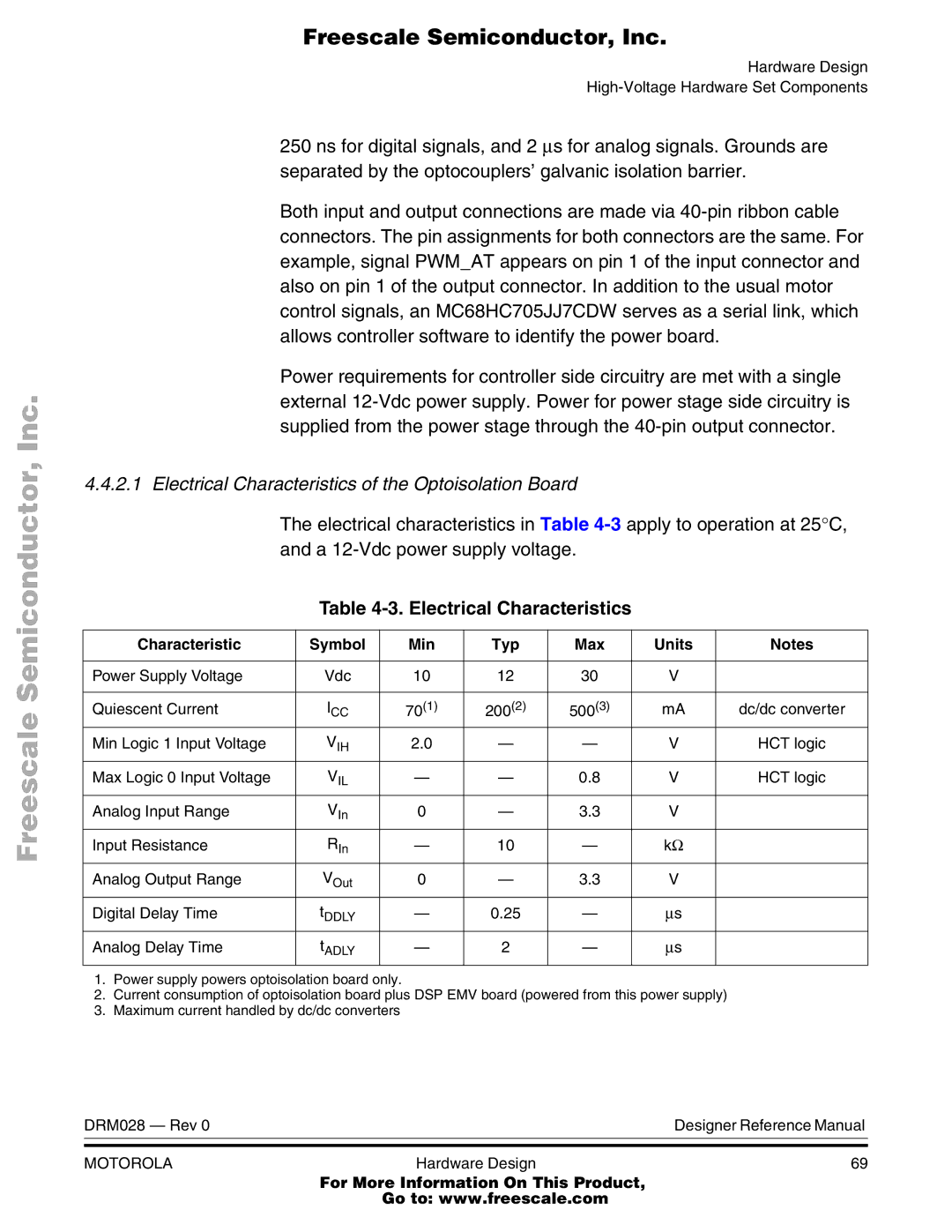
Electrical characteristics in -1apply to operation at 25C
4shows a block diagram of the board’s circuitry
Electrical Characteristics of Control Board
1 3-Phase AC/BLDC High Voltage Power Stage
High-Voltage Hardware Set Components
Phase AC High Voltage Power Stage
Optoisolation Board
Electrical Characteristics of Power Stage
Electrical Characteristics
Electrical Characteristics of the Optoisolation Board
3 3-phase Bldc High Voltage Motor with Motor Brake
Low-Voltage Evaluation Motor Hardware Set Components
EVM Motor Board
Electrical Characteristics of the EVM Motor Board
Electrical Characteristics of the EVM Motor Board
2 3-phase Low Voltage EVM Bldc Motor
Characteristics of the Bldc motor
Low-Voltage Hardware Set Components
1 3-Ph AC/BLDC Low Voltage Power Stage
Block Diagram
Section
2 3-phase Bldc Low Voltage Motor with Motor Brake
Software Design
Data Flow Main Software Flowchart State Diagram
Introduction
Data Flow
Software Variables and Defined Constants
Important system variables are listed in Table
Software Variables
Start/Stop Switch Reading and Start/Stop Decision
Sys3Def
Process Measurement
Process Back, EMF Zero Crossing Sensing
Main Data Flow Part1 Process Fault Control Fault Stop
Freescale Semiconductor, Inc
Main Data Flow Part 2 Alignment, Starting
Closed Loop Control System
Process Desired Speed Setting
Processes Commutation and Zero Crossing Preset and Set
Bldc Speed Control and Calculation
Process Alignment Control
Bldc Commutation and Zero Crossing Selection
Main Software Flowchart
Main Software Flowchart
Freescale Semiconductor, Inc
Main Software Flowchart Main Software Loop
Freescale Semiconductor, Inc
Freescale Semiconductor, Inc
Software Flowchart Interrupts
State Diagram
Application State Transitions
Initialize MCU
State diagram for this software is shown in Figure
Initialize Application
Stand-By
Freescale Semiconductor, Inc
Stand-by State
Align State
Starting Commutation Time Calculation
Freescale Semiconductor, Inc
10. Back-EMF Acquisition
Service of Commutation
Set
Commutation Time Calculation
Service of Received Back-EMF Zero Crossing
Running State
Explained in 5.5.5 Back-EMF Acquisition State
Over Current
11. Running State
Stop State
12. Stop State Fault State
See Figure
Implementation Notes
Software Files
Software files and structure are described in section
Preset Bldc Commutation and Bemf Zero Crossing Selection
Bldc Commutation and Zero Crossing Selection
Set Bldc Commutation and Bemf Zero Crossing Selection
Desired Speed Calculation
Bldc Speed Control and Calculation
PWM Duty Cycle
PWMValMax = DUTYPWMMAX*MCPWMMODULUS
Timer
Timers
Function TIMACh3Int
Designer Reference Manual DRM028 Rev 108 Software Design
Application Suitability Guide
User Guide
Minimal Application Speed
Motor’s nominal speed
Maximal Application Speed
Voltage Closed Loop
Motor Suitability
Mutual Inductance
Designer Reference Manual DRM028 Rev 112 User Guide
Application Hardware and Software Configuration
Hardware Configuration
Hardware setups are shown in -1, -2,
Low-Voltage Evaluation Motor Hardware Set Configuration
High-Voltage Hardware Set Configuration
Low-Voltage Hardware Set Configuration
Controller Board Settings
EVM Board Settings
EVM board settings are the same for all hardware platforms
Software Setup
Application HC08 Software Files
\bldczerocros08MR32\sources\bldc08.c, main program
Application PC Master Software Control Files
Software Execution
Build
Execute from Evaluation Board
Execute from Pre-programmed MCU
When the software is built, the S-record file
Bldczerocros08mr32MMDS.sx is generated
Application Control
PC Master Software Remote Operating Mode
Manual Operating Mode
PC Master Software Control Window
For More Information On This Product
Tuning for Customer Motor
User Guide Tuning for Customer Motor
Follow-up for Software Customizing to Customer Motor
Follow-up for Advanced Software Customizing
Start the PC master software parameters tuning application
To have PC master software installed on your PC computer
11. PC Master Software Parameters Tuning Control Window
Software Parameters Setting Follow-up
Labels in the File const.h
Parameters File Selection
Software Customizing to Power Stage
\bldczerocros08MR32\sources\constcustlv.h, definitions for
Example of Software Customizing to Hardware
Voltage Setting Hardware Customizing
Current Setting Hardware Customizing
Range 0,infinity
Modified maximal measurable voltage is 55 V, so set
Example of Software Customizing to Hardware
Maximal and Minimal Voltage Limits Setting
Software Customizing to Motor Voltage and Current Settings
Detailed description starts here
Range 0,VOLTRANGEMAX
Range 0,CURRENTRANGEMAXA
Maximal and Minimal Current Limits Setting
Alignment Current and Current Regulator Setting
Current during alignment state before motor starts Α
Range 0,8
Parameters Tuning with PC Master Software Project File
Set constcustx.h
From Evaluation Board
12. PC Master Software Current Parameters Tuning Window
Designer Reference Manual DRM028 Rev 142 User Guide
MUSTCHANGEEXPERnn in file constcustx.h
Commutation time period to discharge coil current ∝s
Commutation Parameters
Start-up Constants and Maximal Commutation Period
Start-up Period
Maximal commutation period limit ∝s
Range -128,127
Constcustx.h
Alignment Current and Current Regulator Setting 6.5.4.3
Constcustx.h Set #define Percmtstartus in constcustx.h
Ensure Percmtstartus =PERCMTMAXUS /2
Constcustx.h file
#define Speedpiregigain
13. PC Master Software Start Parameters Tuning Window
Software Customizing to Motor Speed Control Setting
Number of commutations per motor revolution
Range 0,255
Maximal speed range rpm
Minimal speed of the drive rpm
Range 0,SPEEDRANGEMAXRPM
Speedminrpm = 0.07 to 0.5SPEEDMAXRPM
User Guide 153
Execute from Evaluation Board
Set PC master software control mode and start motor see
Remote Operating Mode
Start motor see Application Control and PC Master Software
For the PWM frequency setting, follow the label
PWM Frequency and Current Sampling Period Setting
PWM frequency setting is provided by
PWM Frequency
PWM Frequency Setting
PWM period = Periodpwmus = SETPERPWM*2 EQ
Current Sampling Period
CANCHANGEPERCURSAMPn in const.h file
Conclusion Software Parameters Setting and Tuning
PERCST1US = Periodpwmus * Setpercs ∝s
Current Sampling Instant
User Guide 159
Designer Reference Manual DRM028 Rev 160 User Guide
Appendix A. References
AN1627, Motorola
Motor using MC68HC705MC4 document order number
SG40N
Appendix B. Glossary
Glossary
Serial communications interface module SCI a module that
Designer Reference Manual DRM028 Rev 166 Glossary
Freescale Semiconductor, Inc
HOW to Reach US USA/EUROPE/LOCATIONS not Listed