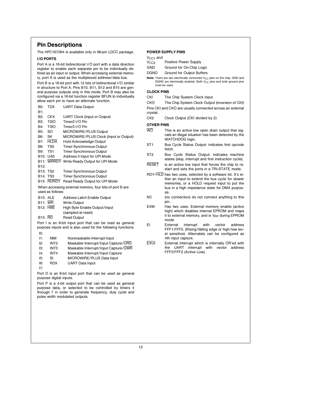
Pin Descriptions
The HPC167064 is available only in
I/O PORTS
Port A is a
Port B is a
B0: | TDX | UART Data Output | |||
B1: |
|
|
|
|
|
B2: | CKX | UART Clock (Input or Output) | |||
B3: | T2IO | Timer2 I/O Pin | |||
B4: | T3IO | Timer3 I/O Pin | |||
B5: | SO | MICROWIRE/PLUS Output | |||
B6: | SK | MICROWIRE/PLUS Clock (Input or Output) | |||
|
|
|
|
|
|
B7: | HLDA | Hold Acknowledge Output | |||
B8: | TS0 | Timer Synchronous Output | |||
B9: | TS1 | Timer Synchronous Output | |||
B10: UA0 | Address 0 Input for UPI Mode | ||||
|
|
|
|
| |
B11: WRRDY | Write Ready Output for UPI Mode | ||||
B12: |
|
|
|
|
|
B13: TS2 | Timer Synchronous Output | ||||
B14: TS3 | Timer Synchronous Output | ||||
|
|
|
| ||
B15: RDRDY | Read Ready Output for UPI Mode | ||||
When accessing external memory, four bits of port B are used as follows:
B10: ALE | Address Latch Enable Output | |||||
|
|
|
|
|
|
|
B11: WR | Write Output | |||||
|
|
|
|
|
| |
B12: HBE | High Byte Enable Output/Input | |||||
|
|
|
|
|
| (sampled at reset) |
|
|
|
| |||
B15: RD | Read Output | |||||
Port I is an
I0: |
|
|
|
|
I1: | NMI | Nonmaskable Interrupt Input | ||
|
|
|
|
|
I2: | INT2 | Maskable Interrupt/Input Capture/URD | ||
|
|
|
| |
I3: | INT3 | Maskable Interrupt/Input Capture/UWR | ||
I4: | INT4 | Maskable Interrupt/Input Capture | ||
I5: | SI | MICROWIRE/PLUS Data Input | ||
I6: | RDX | UART Data Input | ||
I7: |
|
|
|
|
Port D is an
Port P is a
POWER SUPPLY PINS
VCC1 and |
|
VCC2 | Positive Power Supply |
GND | Ground for |
DGND | Ground for Output Buffers |
Note: There are two electrically connected VCC pins on the chip, GND and DGND are electrically isolated. Both VCC pins and both ground pins
| must be used. |
CLOCK PINS | |
CKI | The Chip System Clock Input |
CKO | The Chip System Clock Output (inversion of CKI) |
Pins CKI and CKO are usually connected across an external crystal.
CK2 | Clock Output (CKI divided by 2) | ||
OTHER PINS | |||
|
|
|
|
WO | This is an active low open drain output that sig- | ||
|
|
| nals an illegal situation has been detected by the |
|
|
| WATCHDOG logic. |
ST1 | Bus Cycle Status Output: indicates first opcode | ||
|
|
| fetch. |
ST2 | Bus Cycle Status Output: indicates machine | ||
|
|
| states (skip, interrupt and first instruction cycle). |
|
|
| |
RESET | is an active low input that forces the chip to re- | ||
|
|
| start and sets the ports in a |
RDY/HLD has two uses, selected by a software bit. It’s ei-
|
| ther an input to extend the bus cycle for slower |
|
| memories, or a HOLD request input to put the |
|
| bus in a high impedance state for DMA purpos- |
|
| es. |
NC | (no connection) do not connect anything to this | |
|
| pin. |
EXM | Has two uses. External memory enable (active | |
|
| high) which disables internal EPROM and maps |
|
| it to external memory, and is VPP during EPROM |
|
| mode. |
EI | External interrupt with vector address | |
|
| FFF1:FFF0. (Rising/falling edge or high/low lev- |
|
| el sensitive). Alternately can be configured as |
|
| 4th input capture. |
|
|
|
EXUI | External interrupt which is internally OR’ed with | |
|
| the UART interrupt with vector address |
|
| FFF3:FFF2 (Active Low). |
12
