Design Considerations (Continued)
Designs using the HPC family of
Floating inputs are a frequently overlooked problem. CMOS inputs have extremely high impedance and, if left open, can float to any voltage. You should thus tie unused inputs to VCC or ground, either through a resistor or directly. Unlike the inputs, unused output should be left floating to allow the output to switch without drawing any DC current.
To reduce voltage transients, keep the supply line’s parasit- ic inductances as low as possible by reducing trace lengths, using wide traces, ground planes, and by decoupling the supply with bypass capacitors. In order to prevent additional voltage spiking, this local bypass capacitor must exhibit low inductive reactance. You should therefore use high frequen- cy ceramic capacitors and place them very near the IC to minimize wiring inductance.
XKeep VCC bus routing short. When using double sided or multilayer circuit boards, use ground plane techniques.
XKeep ground lines short, and on PC boards make them as wide as possible, even if trace width varies. Use separate ground traces to supply high current devices such as re- lay and transmission line drivers.
XIn systems mixing linear and logic functions and where supply noise is critical to the analog components’ per- formance, provide separate supply buses or even sepa- rate supplies.
XIf you use local regulators, bypass their inputs with a tan- talum capacitor of at least 1 mF and bypass their outputs with a 10 mF to 50 mF tantalum or aluminum electrolytic capacitor.
XIf the system uses a centralized regulated power supply, use a 10 mF to 20F tantalum electrolytic capacitor or a 50 mF to 100 mF aluminum electrolytic capacitor to de- couple the VCC bus connected to the circuit board.
XProvide localized decoupling. For random logic, a rule of thumb dictates approximately 10 nF (spaced within 12 cm) per every two to five packages, and 100 nF for every 10 packages. You can group these capacitances, but it’s more effective to distribute them among the ICs. If the design has a fair amount of synchronous logic with outputs that tend to switch simultaneously, additional de- coupling might be advisable. Octal
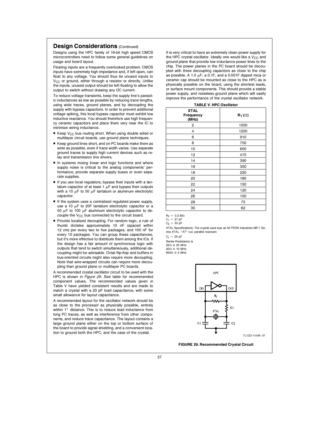
A recommended crystal oscillator circuit to be used with the HPC is shown in Figure 29 . See table for recommended component values. The recommended values given in Table V have yielded consistent results and are made to match a crystal with a 20 pF load capacitance, with some small allowance for layout capacitance.
A recommended layout for the oscillator network should be as close to the processor as physically possible, entirely within 1× distance. This is to reduce lead inductance from long PC traces, as well as interference from other compo- nents, and reduce trace capacitance. The layout contains a large ground plane either on the top or bottom surface of the board to provide signal shielding, and a convenient loca- tion to ground both the HPC, and the case of the crystal.
It is very critical to have an extremely clean power supply for the HPC crystal oscillator. Ideally one would like a VCC and ground plane that provide low inductance power lines to the chip. The power planes in the PC board should be decou- pled with three decoupling capacitors as close to the chip as possible. A 1.0 mF, a 0.1F, and a 0.001F dipped mica or ceramic cap should be mounted as close to the HPC as is physically possible on the board, using the shortest leads, or surface mount components. This should provide a stable power supply, and noiseless ground plane which will vastly improve the performance of the crystal oscillator network.
TABLE V. HPC Oscillator
XTAL |
|
Frequency | R1 (X) |
(MHz) |
|
2 | 1500 |
4 | 1200 |
6 | 910 |
8 | 750 |
10 | 600 |
12 | 470 |
14 | 390 |
16 | 300 |
18 | 220 |
20 | 180 |
22 | 150 |
24 | 120 |
26 | 100 |
28 | 75 |
30 | 62 |
RF e 3.3 MX C1 e 27 pF C2 e 33 pF
XTAL Specifications: The crystal used was an
CL e 20 pF
Series Resistance is 25X @ 25 MHz 40X @ 10 MHz 600X @ 2 MHz
TL/DD/11046 – 37
FIGURE 29. Recommended Crystal Circuit
27
