30 MHz
AC Electrical Characteristics (Continued)
(See Notes 1 and 4 and Figures 1 thru 5 ). VCC e 5V g10%, TA e 0§C to a70§C for HPC467064. (Continued)
| Symbol and Formula |
|
|
|
| Parameter | Min | Max | Units | Notes | ||||||||||||
|
|
|
|
|
|
|
|
|
|
|
|
|
|
|
|
|
|
|
|
|
|
|
| tARR e (/4 tC b 5 |
|
|
|
|
|
|
|
|
|
|
|
|
|
|
|
|
|
|
|
|
|
| ALE Falling Edge to RD Falling Edge | 12 |
| ns |
| |||||||||||||||||
Cycles | tRD e (/2 tC a WS b 39 | Data Input Valid after RD Falling Edge |
| 60 | ns |
| ||||||||||||||||
| tACC e tC a WS b 32 | Data Input Valid after Address Output Valid |
| 100 | ns |
| ||||||||||||||||
Read |
|
|
|
|
|
|
|
|
|
|
|
|
|
|
|
|
|
|
|
|
|
|
tRW e (/2 tC a WS b 14 |
|
|
|
|
|
|
|
|
|
|
|
|
|
|
|
|
|
|
|
|
| |
RD Pulse Width | 85 |
| ns |
| ||||||||||||||||||
|
|
| ||||||||||||||||||||
| tDR e */4 tC b 15 |
|
|
|
|
|
|
|
|
|
|
|
|
|
|
|
|
|
| |||
| Hold of Data Input Valid after RD Rising Edge | 0 | 35 | ns |
| |||||||||||||||||
| tRDA e tC b 15 |
|
|
|
|
|
|
|
|
|
|
|
|
|
|
|
| |||||
| Bus Enable after RD Rising Edge | 51 |
| ns |
| |||||||||||||||||
Cycles | tARW e (/2 tC b 5 |
|
|
|
|
|
|
|
|
|
|
|
|
|
|
| ||||||
ALE Falling Edge to WR Falling Edge | 28 |
| ns |
| ||||||||||||||||||
tWW e */4 tC a WS b 15 |
|
|
|
|
|
|
|
|
|
|
|
|
|
|
|
|
|
|
|
|
| |
WR Pulse Width | 101 |
| ns |
| ||||||||||||||||||
|
|
| ||||||||||||||||||||
Write | tV e (/2 tC a WS b 5 |
|
|
|
|
|
|
|
|
|
|
|
|
|
|
|
|
|
|
|
|
|
Data Output Valid before WR Rising Edge | 94 |
| ns |
| ||||||||||||||||||
|
|
| ||||||||||||||||||||
| tHW e (/4 tC b 10 |
|
|
|
|
|
|
|
|
|
| |||||||||||
| Hold of Data Valid after WR Rising Edge | 7 |
| ns |
| |||||||||||||||||
| tDAR e (/4 tC a WS b 50 |
|
|
|
|
|
|
|
| |||||||||||||
Ready Input | Falling Edge of ALE to Falling Edge of RDY |
| 33 | ns |
| |||||||||||||||||
tRWR e tC |
|
|
|
|
|
|
|
|
|
|
|
|
|
|
|
|
|
|
|
|
| |
RDY Pulse Width | 66 |
| ns |
| ||||||||||||||||||
|
|
| ||||||||||||||||||||
|
|
|
|
|
|
|
|
|
|
|
|
|
|
|
|
|
|
|
|
|
|
|
**This maximum frequency is attainable provided that this external baud clock has a duty cycle such that the high period includes two (2) falling edges of the CK2 clock.
Note: CL e 40 pF.
Note 1: These AC Characteristics are guaranteed with external clock drive on CKI having 50% duty cycle and with less than 15 pF load on CKO with rise and fall times (tCKIR and tCKIL) on CKI input less than 2.5 ns.
Note 2: Do not design with this parameter unless CKI is driven with an active signal. When using a passive crystal circuit, its stability is not guaranteed if either CKI or CKO is connected to any external logic other than the passive components of the crystal circuit.
Note 3: tHAE is spec’d for case with HLD falling edge occurring at the latest time can be accepted during the present CPU cycle being executed. If HLD falling edge occurs later, tHAE may be as long as (3tC a 4 WS a 72tC a 100) depending on the following CPU instruction cycles, its wait states and ready input.
Note 4: WS e tWAIT c (number of
Note 5: Due to emulation
Note 6: Due to tester
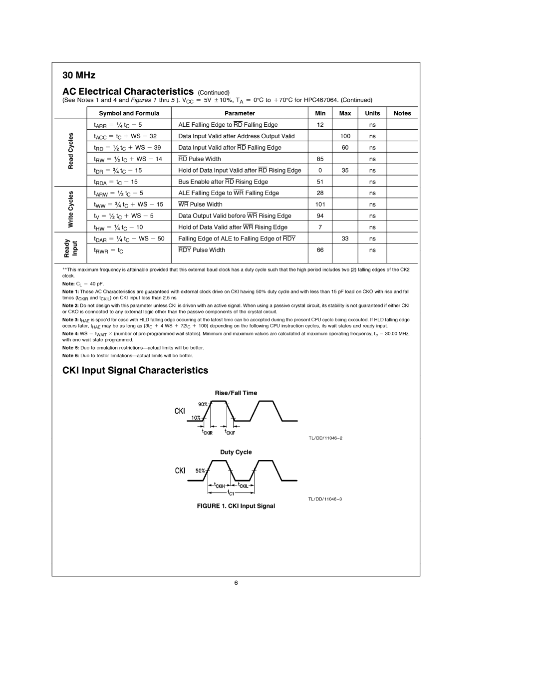
CKI Input Signal Characteristics
Rise/Fall Time
TL/DD/11046 – 2
Duty Cycle
TL/DD/11046 – 3
FIGURE 1. CKI Input Signal
6