Chapter 3
Advanced Chipset Features Setup
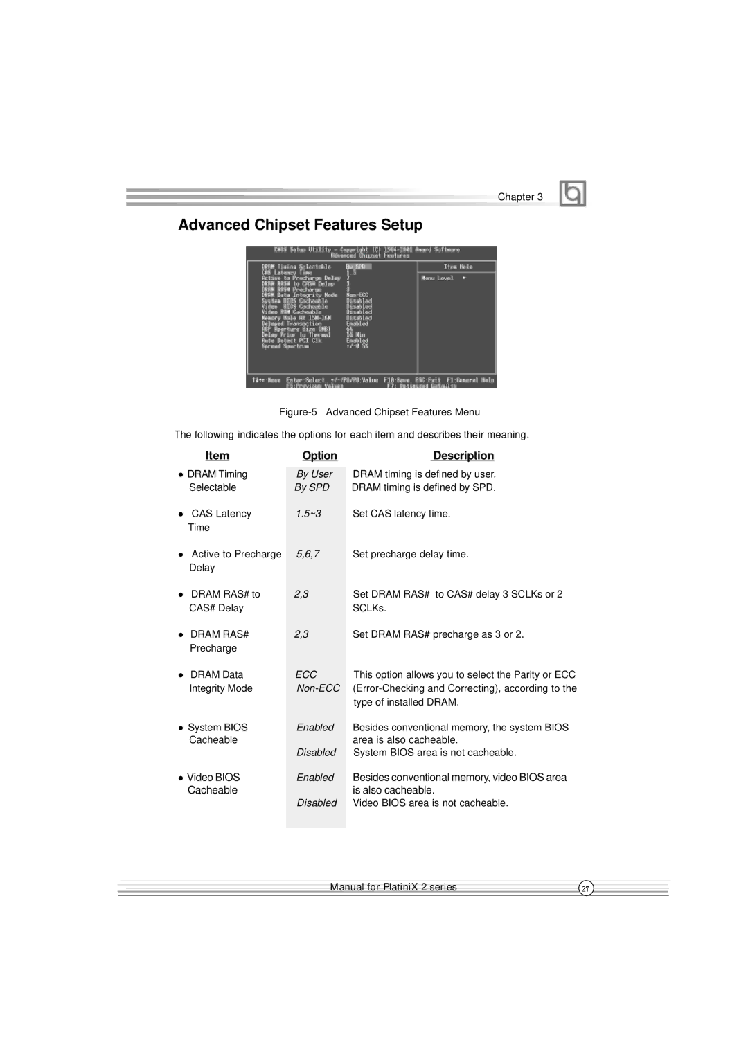
Figure-5 Advanced Chipset Features Menu
The following indicates the options for each item and describes their meaning.
Item
#"DRAM Timing
Selectable
#"CAS Latency Time
#"Active to Precharge Delay
#"DRAM RAS# to CAS# Delay
#"DRAM RAS#
Precharge
#"DRAM Data Integrity Mode
#"System BIOS
Cacheable
#"Video BIOS
Cacheable
Option
By User By SPD
1.5~3
5,6,7
2,3
2,3
ECC
Enabled
Disabled
Enabled
Disabled
Description
DRAM timing is defined by user.
DRAM timing is defined by SPD.
Set CAS latency time.
Set precharge delay time.
Set DRAM RAS# to CAS# delay 3 SCLKs or 2 SCLKs.
Set DRAM RAS# precharge as 3 or 2.
This option allows you to select the Parity or ECC
Besides conventional memory, the system BIOS area is also cacheable.
System BIOS area is not cacheable.
Besides conventional memory, video BIOS area is also cacheable.
Video BIOS area is not cacheable.
![]() Manual for PlatiniX 2 series
Manual for PlatiniX 2 series
