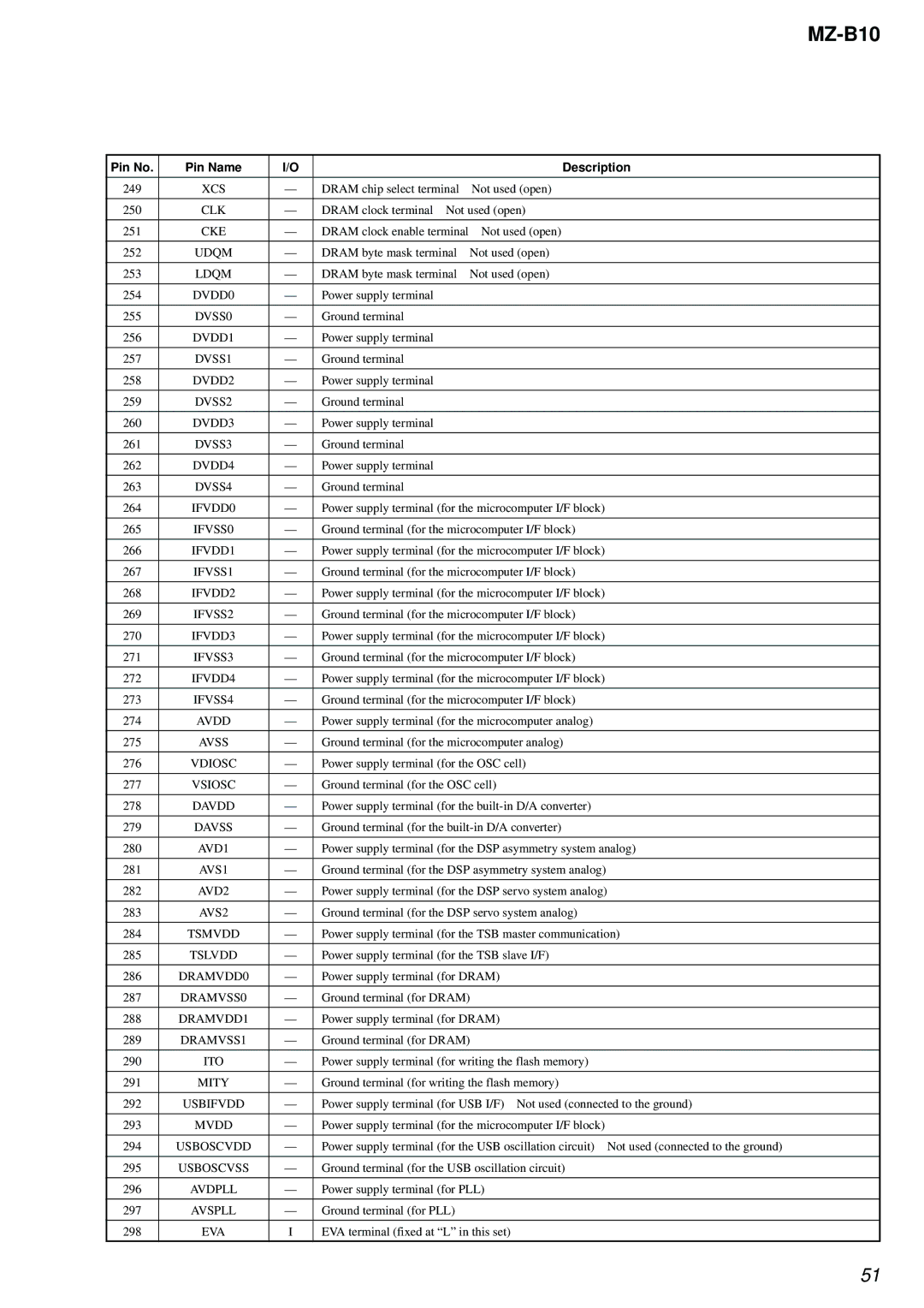
MZ-B10
Pin No. | Pin Name | I/O |
| Description |
|
|
|
|
|
249 | XCS | — | DRAM chip select terminal | Not used (open) |
|
|
|
| |
250 | CLK | — | DRAM clock terminal Not used (open) | |
|
|
|
|
|
251 | CKE | — | DRAM clock enable terminal | Not used (open) |
|
|
|
|
|
252 | UDQM | — | DRAM byte mask terminal | Not used (open) |
|
|
|
|
|
253 | LDQM | — | DRAM byte mask terminal | Not used (open) |
|
|
|
|
|
254 | DVDD0 | — | Power supply terminal |
|
|
|
|
|
|
255 | DVSS0 | — | Ground terminal |
|
|
|
|
|
|
256 | DVDD1 | — | Power supply terminal |
|
|
|
|
|
|
257 | DVSS1 | — | Ground terminal |
|
|
|
|
|
|
258 | DVDD2 | — | Power supply terminal |
|
|
|
|
|
|
259 | DVSS2 | — | Ground terminal |
|
|
|
|
|
|
260 | DVDD3 | — | Power supply terminal |
|
|
|
|
|
|
261 | DVSS3 | — | Ground terminal |
|
|
|
|
|
|
262 | DVDD4 | — | Power supply terminal |
|
|
|
|
|
|
263 | DVSS4 | — | Ground terminal |
|
|
|
|
| |
264 | IFVDD0 | — | Power supply terminal (for the microcomputer I/F block) | |
|
|
|
| |
265 | IFVSS0 | — | Ground terminal (for the microcomputer I/F block) | |
|
|
|
| |
266 | IFVDD1 | — | Power supply terminal (for the microcomputer I/F block) | |
|
|
|
| |
267 | IFVSS1 | — | Ground terminal (for the microcomputer I/F block) | |
|
|
|
| |
268 | IFVDD2 | — | Power supply terminal (for the microcomputer I/F block) | |
|
|
|
| |
269 | IFVSS2 | — | Ground terminal (for the microcomputer I/F block) | |
|
|
|
| |
270 | IFVDD3 | — | Power supply terminal (for the microcomputer I/F block) | |
|
|
|
| |
271 | IFVSS3 | — | Ground terminal (for the microcomputer I/F block) | |
|
|
|
| |
272 | IFVDD4 | — | Power supply terminal (for the microcomputer I/F block) | |
|
|
|
| |
273 | IFVSS4 | — | Ground terminal (for the microcomputer I/F block) | |
|
|
|
| |
274 | AVDD | — | Power supply terminal (for the microcomputer analog) | |
|
|
|
| |
275 | AVSS | — | Ground terminal (for the microcomputer analog) | |
|
|
|
| |
276 | VDIOSC | — | Power supply terminal (for the OSC cell) | |
|
|
|
| |
277 | VSIOSC | — | Ground terminal (for the OSC cell) | |
|
|
|
| |
278 | DAVDD | — | Power supply terminal (for the | |
|
|
|
| |
279 | DAVSS | — | Ground terminal (for the | |
|
|
|
| |
280 | AVD1 | — | Power supply terminal (for the DSP asymmetry system analog) | |
|
|
|
| |
281 | AVS1 | — | Ground terminal (for the DSP asymmetry system analog) | |
|
|
|
| |
282 | AVD2 | — | Power supply terminal (for the DSP servo system analog) | |
|
|
|
| |
283 | AVS2 | — | Ground terminal (for the DSP servo system analog) | |
|
|
|
| |
284 | TSMVDD | — | Power supply terminal (for the TSB master communication) | |
|
|
|
| |
285 | TSLVDD | — | Power supply terminal (for the TSB slave I/F) | |
|
|
|
| |
286 | DRAMVDD0 | — | Power supply terminal (for DRAM) | |
|
|
|
| |
287 | DRAMVSS0 | — | Ground terminal (for DRAM) | |
|
|
|
| |
288 | DRAMVDD1 | — | Power supply terminal (for DRAM) | |
|
|
|
| |
289 | DRAMVSS1 | — | Ground terminal (for DRAM) | |
|
|
|
| |
290 | ITO | — | Power supply terminal (for writing the flash memory) | |
|
|
|
| |
291 | MITY | — | Ground terminal (for writing the flash memory) | |
|
|
|
| |
292 | USBIFVDD | — | Power supply terminal (for USB I/F) Not used (connected to the ground) | |
|
|
|
| |
293 | MVDD | — | Power supply terminal (for the microcomputer I/F block) | |
|
|
|
| |
294 | USBOSCVDD | — | Power supply terminal (for the USB oscillation circuit) Not used (connected to the ground) | |
|
|
|
| |
295 | USBOSCVSS | — | Ground terminal (for the USB oscillation circuit) | |
|
|
|
| |
296 | AVDPLL | — | Power supply terminal (for PLL) | |
|
|
|
|
|
297 | AVSPLL | — | Ground terminal (for PLL) |
|
|
|
|
| |
298 | EVA | I | EVA terminal (fixed at “L” in this set) | |
|
|
|
|
|
51