MZ-B10
Ver 1.2 2003.09
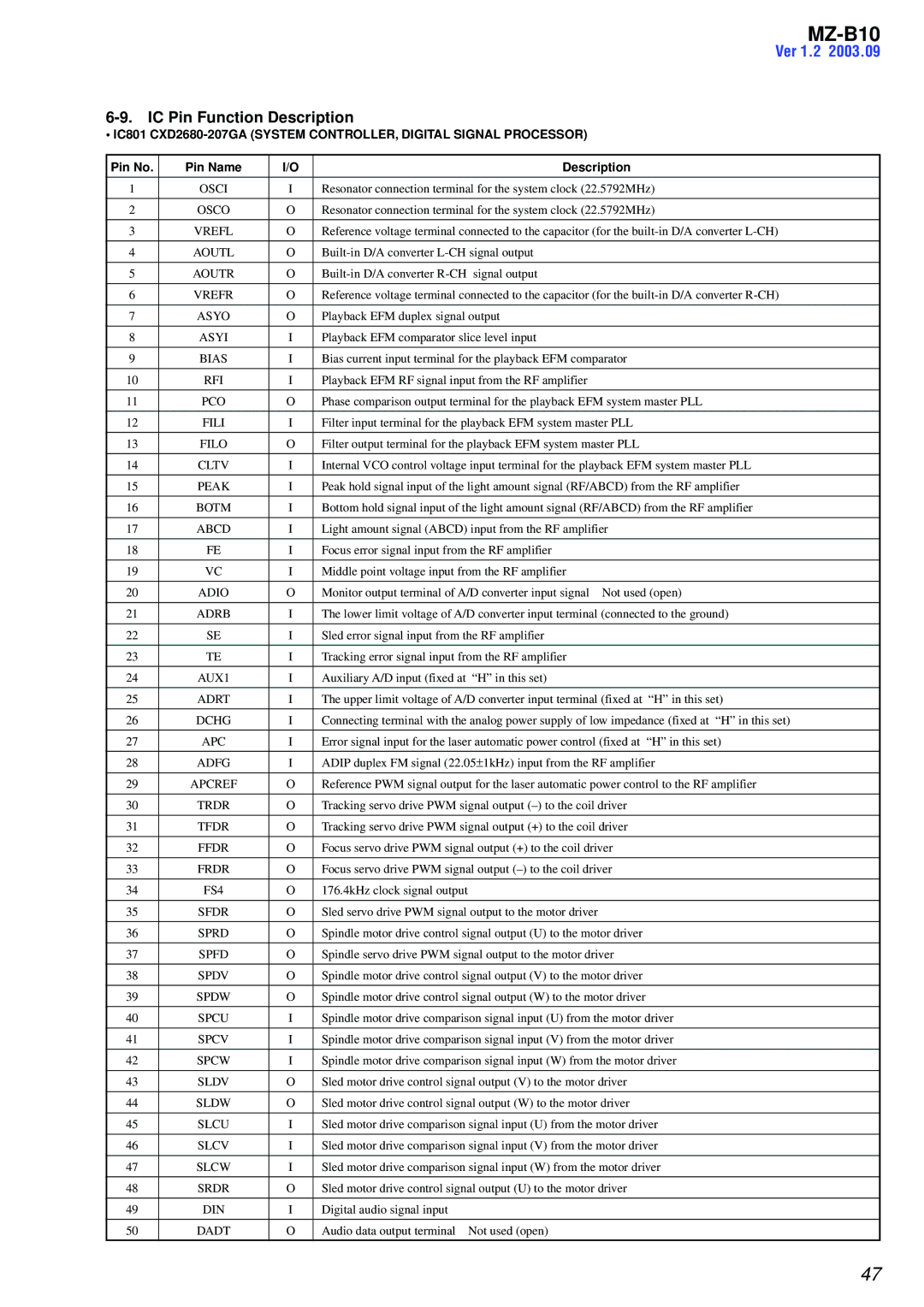
6-9. IC Pin Function Description
• IC801
Pin No. | Pin Name | I/O |
| Description |
|
|
|
| |
1 | OSCI | I | Resonator connection terminal for the system clock (22.5792MHz) | |
|
|
|
| |
2 | OSCO | O | Resonator connection terminal for the system clock (22.5792MHz) | |
|
|
|
| |
3 | VREFL | O | Reference voltage terminal connected to the capacitor (for the | |
|
|
|
| |
4 | AOUTL | O | ||
|
|
|
| |
5 | AOUTR | O | ||
|
|
|
| |
6 | VREFR | O | Reference voltage terminal connected to the capacitor (for the | |
|
|
|
| |
7 | ASYO | O | Playback EFM duplex signal output | |
|
|
|
| |
8 | ASYI | I | Playback EFM comparator slice level input | |
|
|
|
| |
9 | BIAS | I | Bias current input terminal for the playback EFM comparator | |
|
|
|
| |
10 | RFI | I | Playback EFM RF signal input from the RF amplifier | |
|
|
|
| |
11 | PCO | O | Phase comparison output terminal for the playback EFM system master PLL | |
|
|
|
| |
12 | FILI | I | Filter input terminal for the playback EFM system master PLL | |
|
|
|
| |
13 | FILO | O | Filter output terminal for the playback EFM system master PLL | |
|
|
|
| |
14 | CLTV | I | Internal VCO control voltage input terminal for the playback EFM system master PLL | |
|
|
|
| |
15 | PEAK | I | Peak hold signal input of the light amount signal (RF/ABCD) from the RF amplifier | |
|
|
|
| |
16 | BOTM | I | Bottom hold signal input of the light amount signal (RF/ABCD) from the RF amplifier | |
|
|
|
| |
17 | ABCD | I | Light amount signal (ABCD) input from the RF amplifier | |
|
|
|
| |
18 | FE | I | Focus error signal input from the RF amplifier | |
|
|
|
| |
19 | VC | I | Middle point voltage input from the RF amplifier | |
|
|
|
| |
20 | ADIO | O | Monitor output terminal of A/D converter input signal Not used (open) | |
|
|
|
| |
21 | ADRB | I | The lower limit voltage of A/D converter input terminal (connected to the ground) | |
|
|
|
| |
22 | SE | I | Sled error signal input from the RF amplifier | |
|
|
|
| |
23 | TE | I | Tracking error signal input from the RF amplifier | |
|
|
|
|
|
24 | AUX1 | I | Auxiliary A/D input (fixed at | “H” in this set) |
|
|
|
| |
25 | ADRT | I | The upper limit voltage of A/D converter input terminal (fixed at “H” in this set) | |
|
|
|
| |
26 | DCHG | I | Connecting terminal with the analog power supply of low impedance (fixed at “H” in this set) | |
|
|
|
| |
27 | APC | I | Error signal input for the laser automatic power control (fixed at “H” in this set) | |
|
|
|
| |
28 | ADFG | I | ADIP duplex FM signal (22.05±1kHz) input from the RF amplifier | |
|
|
|
| |
29 | APCREF | O | Reference PWM signal output for the laser automatic power control to the RF amplifier | |
|
|
|
| |
30 | TRDR | O | Tracking servo drive PWM signal output | |
|
|
|
| |
31 | TFDR | O | Tracking servo drive PWM signal output (+) to the coil driver | |
|
|
|
| |
32 | FFDR | O | Focus servo drive PWM signal output (+) to the coil driver | |
|
|
|
| |
33 | FRDR | O | Focus servo drive PWM signal output | |
|
|
|
|
|
34 | FS4 | O | 176.4kHz clock signal output |
|
|
|
|
| |
35 | SFDR | O | Sled servo drive PWM signal output to the motor driver | |
|
|
|
| |
36 | SPRD | O | Spindle motor drive control signal output (U) to the motor driver | |
|
|
|
| |
37 | SPFD | O | Spindle servo drive PWM signal output to the motor driver | |
|
|
|
| |
38 | SPDV | O | Spindle motor drive control signal output (V) to the motor driver | |
|
|
|
| |
39 | SPDW | O | Spindle motor drive control signal output (W) to the motor driver | |
|
|
|
| |
40 | SPCU | I | Spindle motor drive comparison signal input (U) from the motor driver | |
|
|
|
| |
41 | SPCV | I | Spindle motor drive comparison signal input (V) from the motor driver | |
|
|
|
| |
42 | SPCW | I | Spindle motor drive comparison signal input (W) from the motor driver | |
|
|
|
| |
43 | SLDV | O | Sled motor drive control signal output (V) to the motor driver | |
|
|
|
| |
44 | SLDW | O | Sled motor drive control signal output (W) to the motor driver | |
|
|
|
| |
45 | SLCU | I | Sled motor drive comparison signal input (U) from the motor driver | |
|
|
|
| |
46 | SLCV | I | Sled motor drive comparison signal input (V) from the motor driver | |
|
|
|
| |
47 | SLCW | I | Sled motor drive comparison signal input (W) from the motor driver | |
|
|
|
| |
48 | SRDR | O | Sled motor drive control signal output (U) to the motor driver | |
|
|
|
|
|
49 | DIN | I | Digital audio signal input |
|
|
|
|
|
|
50 | DADT | O | Audio data output terminal | Not used (open) |
|
|
|
|
|
47