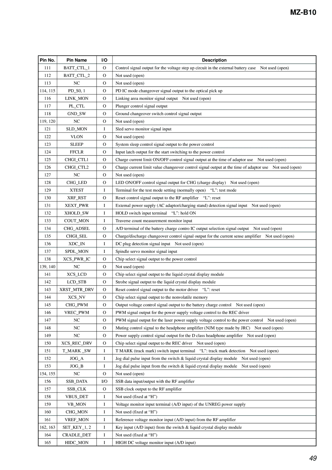
MZ-B10
Pin No. | Pin Name | I/O |
|
| Description |
|
|
|
|
|
|
|
|
|
| ||||||
111 | BATT_CTL_1 | O | Control signal output for the voltage step up circuit in the external battery case | Not used (open) | ||||||
|
|
|
|
|
|
|
|
|
|
|
112 | BATT_CTL_2 | O | Not used (open) |
|
|
|
|
|
|
|
|
|
|
|
|
|
|
|
|
|
|
113 | NC | O | Not used (open) |
|
|
|
|
|
|
|
|
|
|
|
|
|
|
|
| ||
114, 115 | PD_S0, 1 | O | PD IC mode changeover signal output to the optical pick up |
|
|
|
|
| ||
|
|
|
|
|
|
|
|
| ||
116 | LINK_MON | O | Linking area monitor signal output Not used (open) |
|
|
|
|
| ||
|
|
|
|
|
|
|
|
|
|
|
117 | PL_CTL | O | Plunger control signal output |
|
|
|
|
|
|
|
|
|
|
|
|
|
|
|
| ||
118 | GND_SW | O | Ground changeover switch control signal output |
|
|
|
|
| ||
|
|
|
|
|
|
|
|
|
|
|
119, 120 | NC | O | Not used (open) |
|
|
|
|
|
|
|
|
|
|
|
|
|
|
|
|
|
|
121 | SLD_MON | I | Sled servo monitor signal input |
|
|
|
|
|
|
|
|
|
|
|
|
|
|
|
|
|
|
122 | VLON | O | Not used (open) |
|
|
|
|
|
|
|
|
|
|
|
|
|
|
|
| ||
123 | SLEEP | O | System sleep control signal output to the power control |
|
|
|
|
| ||
|
|
|
|
|
|
|
|
| ||
124 | FFCLR | O | Input latch output for the start switching to the power control |
|
|
|
|
| ||
|
|
|
|
| ||||||
125 | CHGI_CTL1 | O | Charge current limit ON/OFF control signal output at the time of adaptor use | Not used (open) | ||||||
|
|
|
| |||||||
126 | CHGI_CTL2 | O | Charge current limit value changeover control signal output at the time of adaptor use Not used (open) | |||||||
|
|
|
|
|
|
|
|
|
|
|
127 | NC | O | Not used (open) |
|
|
|
|
|
|
|
|
|
|
|
| ||||||
128 | CHG_LED | O | LED ON/OFF control signal output for CHG (charge display) Not used (open) |
| ||||||
|
|
|
|
|
|
|
|
| ||
129 | XTEST | I | Terminal for the test mode setting (normally open) “L”: test mode |
|
|
|
|
| ||
|
|
|
|
|
|
|
|
|
| |
130 | XRF_RST | O | Reset control signal output to the RF amplifier | “L”: reset |
|
|
|
|
| |
|
|
|
|
| ||||||
131 | XEXT_PWR | I | External power supply (AC adaptor/charging stand) detection signal input | Not used (open) | ||||||
|
|
|
|
|
|
|
|
|
|
|
132 | XHOLD_SW | I | HOLD switch input terminal | “L”: hold ON |
|
|
|
|
|
|
|
|
|
|
|
|
|
|
|
| |
133 | COUT_MON | I | Traverse count measurement monitor input |
|
|
|
|
|
| |
|
|
|
|
| ||||||
134 | CHG_ADSEL | O | A/D terminal of the battery charge contro IC output selection signal output | Not used (open) | ||||||
|
|
|
|
| ||||||
135 | CHGI_SEL | O | Charge/discharge changeover control signal output for the current sense amplifier | Not used (open) | ||||||
|
|
|
|
|
|
|
|
|
| |
136 | XDC_IN | I | DC plug detection signal input | Not used (open) |
|
|
|
|
| |
|
|
|
|
|
|
|
|
|
| |
137 | SPDL_MON | I | Spindle servo monitor signal input |
|
|
|
|
|
| |
|
|
|
|
|
|
|
|
|
| |
138 | XCS_PWR_IC | O | Chip select signal output to the power control |
|
|
|
|
|
| |
|
|
|
|
|
|
|
|
|
|
|
139, 140 | NC | O | Not used (open) |
|
|
|
|
|
|
|
|
|
|
|
|
|
|
|
| ||
141 | XCS_LCD | O | Chip select signal output to the liquid crystal display module |
|
|
|
|
| ||
|
|
|
|
|
|
|
|
| ||
142 | LCD_STB | O | Strobe signal output to the liquid crystal display module |
|
|
|
|
| ||
|
|
|
|
|
|
|
|
|
| |
143 | XRST_MTR_DRV | O | Reset control signal output to the motor driver | “L”: reset |
|
|
|
|
| |
|
|
|
|
|
|
|
|
| ||
144 | XCS_NV | O | Chip select signal output to the nonvolatile memory |
|
|
|
|
| ||
|
|
|
|
| ||||||
145 | CHG_PWM | O | Output voltage control signal output to the battery charge control Not used (open) |
| ||||||
|
|
|
|
|
|
| ||||
146 | VREC_PWM | O | PWM signal output for the power supply voltage control to the REC driver |
|
|
| ||||
|
|
|
|
| ||||||
147 | NC | O | PWM signal output for the laser power supply voltage control to the power control | Not used (open) | ||||||
|
|
|
|
| ||||||
148 | NC | O | Muting control signal to the headphone amplifier (NJM type made by JRC) | Not used (open) | ||||||
|
|
|
|
| ||||||
149 | NC | O | Power supply control signal output for the D class headphone amplifier | Not used (open) | ||||||
|
|
|
|
|
|
|
|
| ||
150 | XCS_REC_DRV | O | Chip select signal output to the REC driver Not used (open) |
|
|
|
|
| ||
|
|
|
|
|
| |||||
151 | T_MARK _SW | I | T MARK (track mark) switch input terminal | “L”: track mark detection | Not used (open) | |||||
|
|
|
|
| ||||||
152 | JOG_A | I | Jog dial pulse input from the switch & liquid crystal display module | Not used (open) | ||||||
|
|
|
|
| ||||||
153 | JOG_B | I | Jog dial pulse input from the switch & liquid crystal display module | Not used (open) | ||||||
|
|
|
|
|
|
|
|
|
|
|
154, 155 | NC | O | Not used (open) |
|
|
|
|
|
|
|
|
|
|
|
|
|
|
|
|
| |
156 | SSB_DATA | I/O | SSB data input/output with the RF amplifier |
|
|
|
|
|
| |
|
|
|
|
|
|
|
|
|
| |
157 | SSB_CLK | O | SSB clock output to the RF amplifier |
|
|
|
|
|
| |
|
|
|
|
|
|
|
|
|
|
|
158 | VBUS_DET | I | Not used (fixed at “H”) |
|
|
|
|
|
|
|
|
|
|
|
|
|
|
| |||
159 | VB_MON | I | Voltage monitor input terminal (A/D input) of the UNREG power supply |
|
|
|
| |||
|
|
|
|
|
|
|
|
|
|
|
160 | CHG_MON | I | Not used (fixed at “H”) |
|
|
|
|
|
|
|
|
|
|
|
|
|
|
|
| ||
161 | VREF_MON | I | Reference voltage monitor input (A/D input) from the RF amplifier |
|
|
|
|
| ||
|
|
|
|
|
|
|
| |||
162, 163 | SET_KEY_1, 2 | I | Key input (A/D input) from the switch & liquid crystal display module |
|
|
|
| |||
|
|
|
|
|
|
|
|
|
|
|
164 | CRADLE_DET | I | Not used (fixed at “H”) |
|
|
|
|
|
|
|
|
|
|
|
|
|
|
|
|
| |
165 | HIDC_MON | I | HIGH DC voltage monitor input (A/D input) |
|
|
|
|
|
| |
|
|
|
|
|
|
|
|
|
|
|
49