(Page 30)
(Page 33)
(Page 33)
(Page 36)
– 31 –
(Page 34)
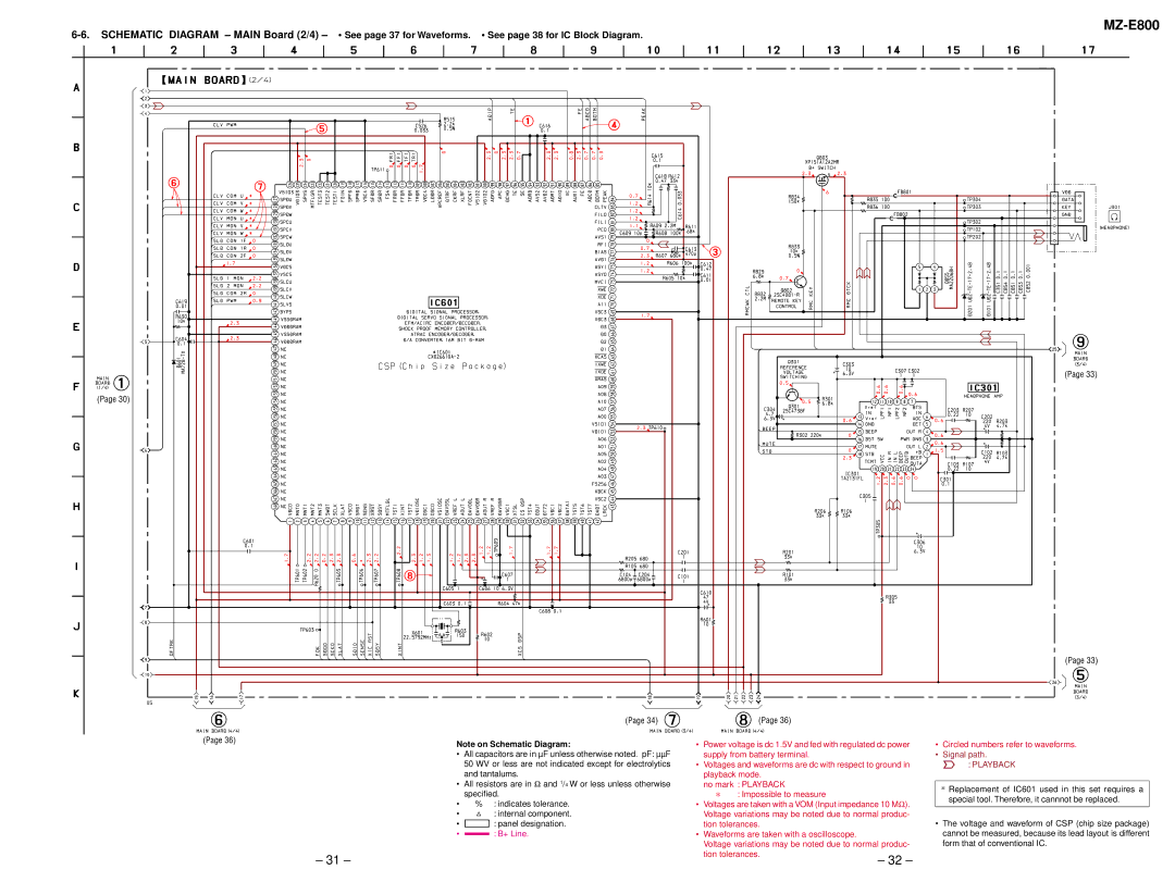
Note on Schematic Diagram:
•All capacitors are in µF unless otherwise noted. pF: µµF 50 WV or less are not indicated except for electrolytics and tantalums.
•All resistors are in Ω and 1/4 W or less unless otherwise specified.
•% : indicates tolerance.
•f : internal component.
•C: panel designation.
•A : B+ Line.
(Page 36)
•Power voltage is dc 1.5V and fed with regulated dc power supply from battery terminal.
•Voltages and waveforms are dc with respect to ground in playback mode.
no mark : PLAYBACK
∗: Impossible to measure
•Voltages are taken with a VOM (Input impedance 10 MΩ ). Voltage variations may be noted due to normal produc- tion tolerances.
•Waveforms are taken with a oscilloscope.
Voltage variations may be noted due to normal produc- tion tolerances.
•Circled numbers refer to waveforms.
•Signal path.
E : PLAYBACK
*Replacement of IC601 used in this set requires a special tool. Therefore, it cannnot be replaced.
•The voltage and waveform of CSP (chip size package) cannot be measured, because its lead layout is different form that of conventional IC.
