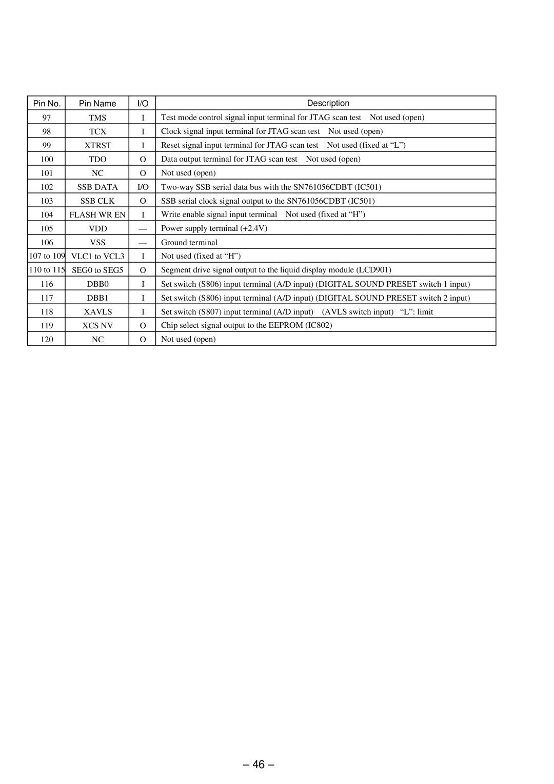
Pin No. | Pin Name | I/O | Description | |
|
|
|
| |
97 | TMS | I | Test mode control signal input terminal for JTAG scan test Not used (open) | |
|
|
|
|
|
98 | TCX | I | Clock signal input terminal for JTAG scan test | Not used (open) |
|
|
|
|
|
99 | XTRST | I | Reset signal input terminal for JTAG scan test | Not used (fixed at “L”) |
|
|
|
| |
100 | TDO | O | Data output terminal for JTAG scan test Not used (open) | |
|
|
|
|
|
101 | NC | O | Not used (open) |
|
102 | SSB DATA | I/O | ||
103 | SSB CLK | O | SSB serial clock signal output to the SN761056CDBT (IC501) | |
|
|
|
| |
104 | FLASH WR EN | I | Write enable signal input terminal Not used (fixed at “H”) | |
|
|
|
|
|
105 | VDD | — | Power supply terminal (+2.4V) |
|
|
|
|
|
|
106 | VSS | — | Ground terminal |
|
|
|
|
|
|
107 to 109 | VLC1 to VCL3 | I | Not used (fixed at “H”) |
|
110 to 115 | SEG0 to SEG5 | O | Segment drive signal output to the liquid display module (LCD901) | |
116 | DBB0 | I | Set switch (S806) input terminal (A/D input) (DIGITAL SOUND PRESET switch 1 input) | |
|
|
|
| |
117 | DBB1 | I | Set switch (S806) input terminal (A/D input) (DIGITAL SOUND PRESET switch 2 input) | |
|
|
|
|
|
118 | XAVLS | I | Set switch (S807) input terminal (A/D input) | (AVLS switch input) “L”: limit |
|
|
|
| |
119 | XCS NV | O | Chip select signal output to the EEPROM (IC802) | |
|
|
|
|
|
120 | NC | O | Not used (open) |
|
– 46 –