![]()
![]()
![]()
![]() X7DBi+ User's Manual
X7DBi+ User's Manual
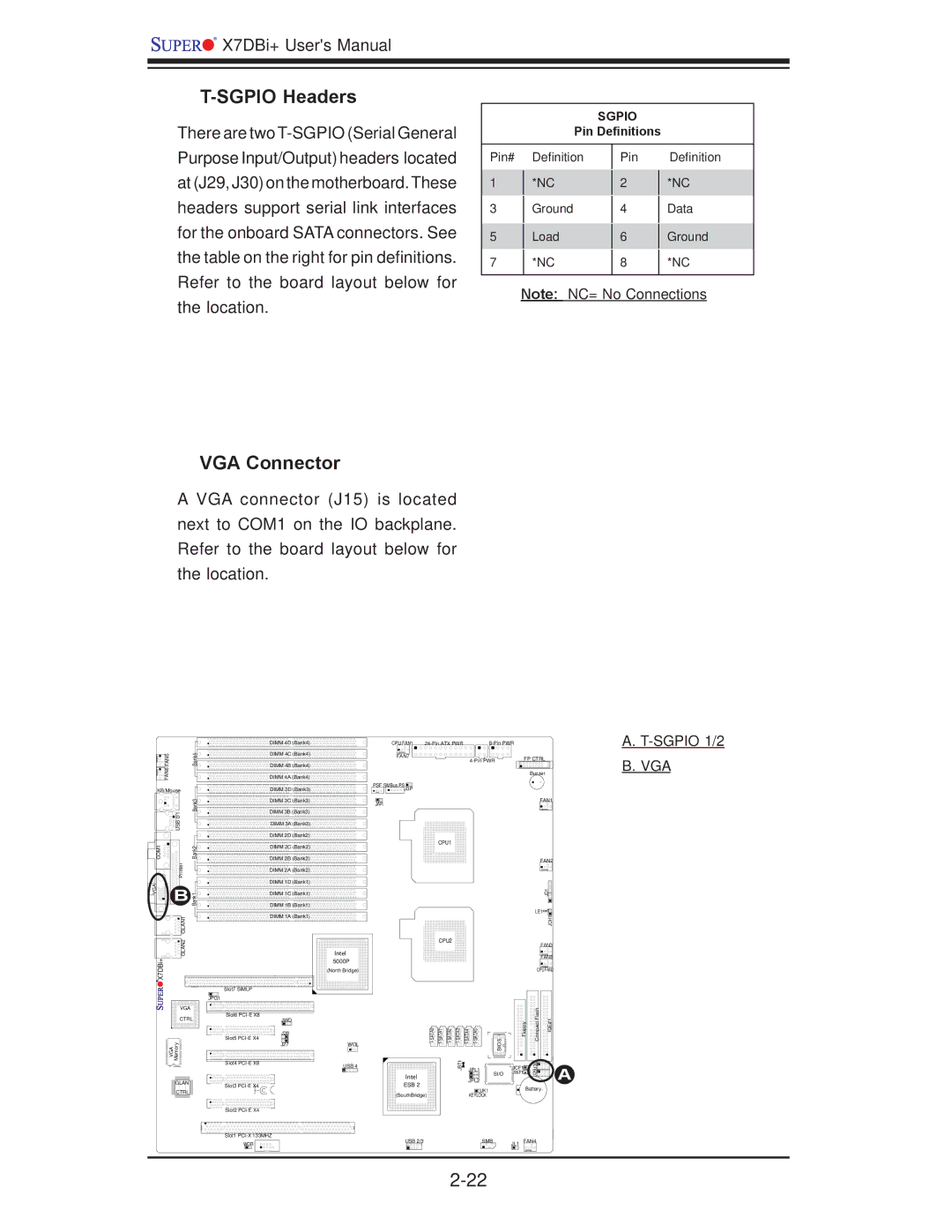
T-SGPIO Headers
There are two T-SGPIO (Serial General
SGPIO
Pin Definitions
Purpose Input/Output) headers located at (J29, J30) on the motherboard. These headers support serial link interfaces for the onboard SATA connectors. See the table on the right for pin definitions. Refer to the board layout below for
Pin# |
| Definition |
1 |
| *NC |
| ||
3 |
| Ground |
| ||
5 |
| Load |
| ||
7 |
| *NC |
| ||
|
|
|
Pin
2
4
6
8
Definition
*NC
Data
Ground
*NC
the location.
Note: NC= No Connections
VGA Connector
A VGA connector (J15) is located next to COM1 on the IO backplane. Refer to the board layout below for the location.
|
| DIMM 4D (Bank4) | |
FAN5 | Bank4 | DIMM 4C (Bank4) | |
DIMM 4B (Bank4) | |||
FAN6 |
| ||
| DIMM 4A (Bank4) | ||
KB/Mouse |
| DIMM 3D (Bank3) |
CPU FAN1 |
| |
FAN7 | FP CTRL | |
| ||
|
| |
|
| Buzzer |
PSF SMBus PSJ3P
A.T-SGPIO 1/2
B.VGA
Bank3 |
USB 0/1 |
DIMM 3C![]() (Bank3)
(Bank3)
DIMM 3B![]() (Bank3)
(Bank3)
DIMM 3A (Bank3)
DIMM 2D![]() (Bank2)
(Bank2)
JAR
FAN1
COM1 | Bank2 |
| Printer |
VGA | B Bank1 |
| GLAN1 |
DIMM 2C (Bank2)
DIMM 2B![]() (Bank2)
(Bank2)
DIMM 2A![]() (Bank2)
(Bank2)
DIMM 1D![]() (Bank1)
(Bank1)
DIMM 1C![]() (Bank1)
(Bank1)
DIMM 1B![]() (Bank1)
(Bank1)
DIMM 1A![]() (Bank1)
(Bank1)
CPU1
FAN2
JD1![]()
LE1![]()
![]()
JOH1
GLAN2 |
Intel |
CPU2 |
FAN3 |
FAN8 |
X7DBi+
| Slot7 SIMLP | |
| JPG1 | |
VGA |
| |
CTRL | Slot6 | |
JWD | ||
| J28 | |
VGA Memory | Slot5 | |
J27 | ||
Slot4 | ||
| ||
GLAN | Slot3 | |
CTRL | ||
| ||
| Slot2 | |
| Slot1 |
5000P |
(North Bridge) |
WOL
USB 4
|
|
|
| CPU FAN2 | |
BIOS | Floppy | Compact Flash | IDE#1 | ||
JBT1 | SI/O | JWF1 | J29J30 |
| JPL1 | JCF1 |
|
|
|
| |
Intel | JPL2 |
|
|
ESB 2 |
|
| |
JK1 |
| Battery | |
(SouthBridge) |
| ||
KEYLOCK |
|
|
A
WOR |
USB 2/3 | SMB | JL1 FAN4 |