TS32M~1GCF80 | 80X CompactFlash Card | |
|
|
|
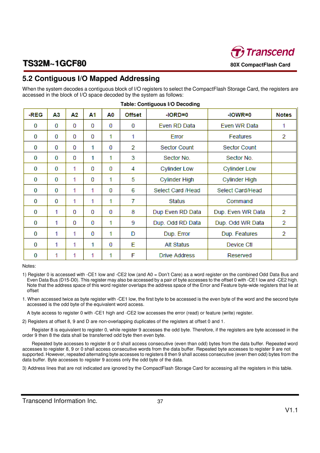
5.2 Contiguous I/O Mapped Addressing
When the system decodes a contiguous block of I/O registers to select the CompactFlash Storage Card, the registers are accessed in the block of I/O space decoded by the system as follows:
Table: Contiguous I/O Decoding
Notes:
1)Register 0 is accessed with
1.When accessed twice as byte register with
A byte access to register 0 with
2) Registers at offset 8, 9 and D are
Register 8 is equivalent to register 0, while register 9 accesses the odd byte. Therefore, if the registers are byte accessed in the order 9 then 8 the data shall be transferred odd byte then even byte.
Repeated byte accesses to register 8 or 0 shall access consecutive (even than odd) bytes from the data buffer. Repeated word accesses to register 8, 9 or 0 shall access consecutive words from the data buffer. Repeated byte accesses to register 9 are not supported. However, repeated alternating byte accesses to registers 8 then 9 shall access consecutive (even then odd) bytes from the data buffer. Byte accesses to register 9 access only the odd byte of the data.
3) Address lines that are not indicated are ignored by the CompactFlash Storage Card for accessing all the registers in this table.
Transcend Information Inc. | 37 |