TS32M~1GCF80 | 80X CompactFlash Card | |
|
|
|
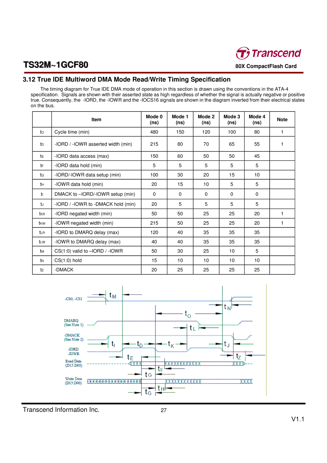
3.12 True IDE Multiword DMA Mode Read/Write Timing Specification
The timing diagram for True IDE DMA mode of operation in this section is drawn using the conventions in the
| Item | Mode 0 | Mode 1 | Mode 2 | Mode 3 | Mode 4 | |
| (ns) | (ns) | (ns) | (ns) | (ns) | ||
|
| ||||||
|
|
|
|
|
|
| |
tO | Cycle time (min) | 480 | 150 | 120 | 100 | 80 | |
tD | 215 | 80 | 70 | 65 | 55 | ||
tE | 150 | 60 | 50 | 50 | 45 | ||
tF | 5 | 5 | 5 | 5 | 5 | ||
tG | 100 | 30 | 20 | 15 | 10 | ||
tH | 20 | 15 | 10 | 5 | 5 | ||
tI | DMACK to | 0 | 0 | 0 | 0 | 0 | |
tJ | 20 | 5 | 5 | 5 | 5 | ||
|
|
|
|
|
|
| |
tKR | 50 | 50 | 25 | 25 | 20 | ||
|
|
|
|
|
|
| |
tKW | 215 | 50 | 25 | 25 | 20 | ||
tLR | 120 | 40 | 35 | 35 | 35 | ||
tLW | 40 | 40 | 35 | 35 | 35 | ||
tM | CS(1:0) valid to | 50 | 30 | 25 | 10 | 5 | |
tN | CS(1:0) hold | 15 | 10 | 10 | 10 | 10 | |
|
|
|
|
|
|
| |
tZ |
| 20 | 25 | 25 | 25 | 25 | |
|
|
|
|
|
|
|
Note
1
1
1
1
Transcend Information Inc. | 27 |