TS32M~1GCF80 | 80X CompactFlash Card | |
|
|
|
Note: Because of the overlapped registers, PC Card modes access to the 1F1h, 171h or offset 1 are not defined for word
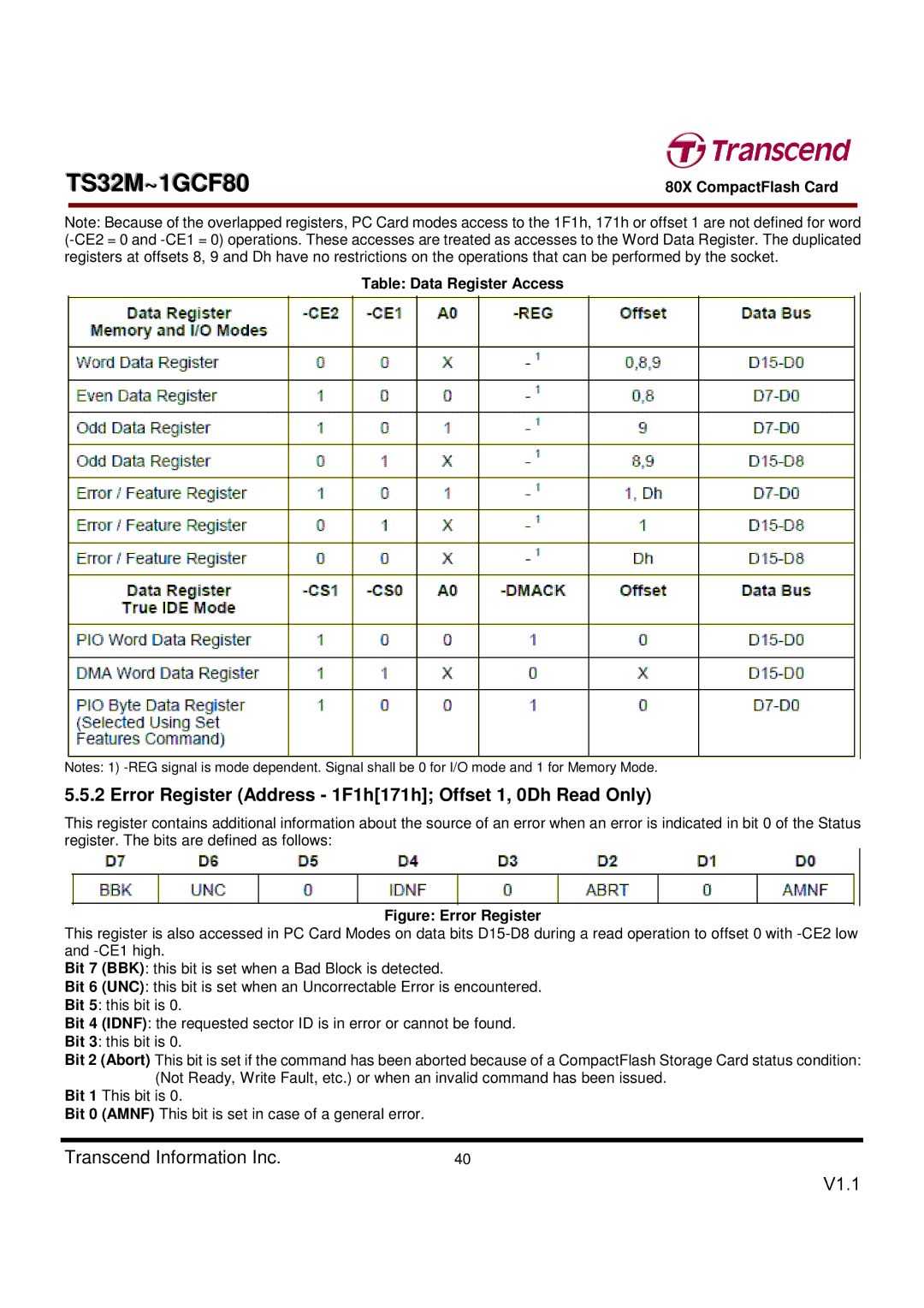
Table: Data Register Access
Notes: 1)
5.5.2 Error Register (Address - 1F1h[171h]; Offset 1, 0Dh Read Only)
This register contains additional information about the source of an error when an error is indicated in bit 0 of the Status register. The bits are defined as follows:
Figure: Error Register
This register is also accessed in PC Card Modes on data bits
Bit 7 (BBK): this bit is set when a Bad Block is detected.
Bit 6 (UNC): this bit is set when an Uncorrectable Error is encountered.
Bit 5: this bit is 0.
Bit 4 (IDNF): the requested sector ID is in error or cannot be found.
Bit 3: this bit is 0.
Bit 2 (Abort) This bit is set if the command has been aborted because of a CompactFlash Storage Card status condition: (Not Ready, Write Fault, etc.) or when an invalid command has been issued.
Bit 1 This bit is 0.
Bit 0 (AMNF) This bit is set in case of a general error.
Transcend Information Inc. | 40 |