T
T
TS
S
S3
3
32
2
2M
M
M~
~
~1
1
1G
G
GC
C
CF
F
F8
8
80
0
0
80X CompactFlash Card
Transcend Information Inc.
36
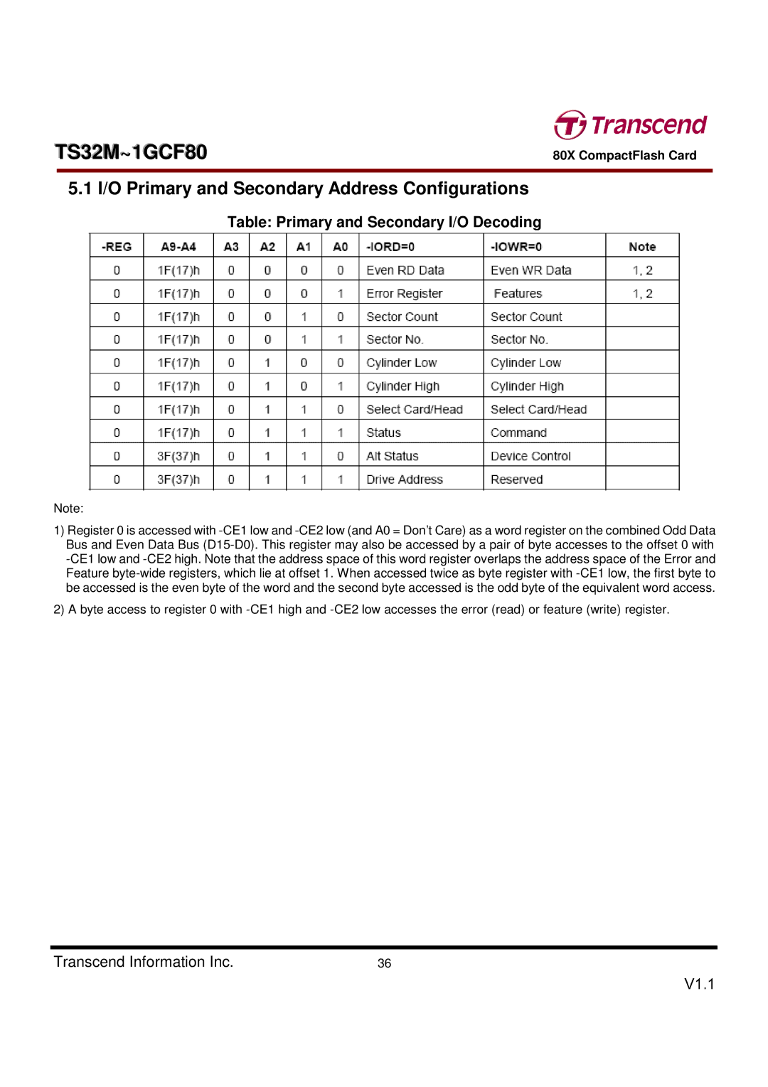
5.1 I/O Primary and Secondary Address Configurations
Table: Primary and Secondary I/O Decoding
Note:
1) Register 0 is accessed with -CE1 low and -CE2 low (and A0 = Don’t Care) as a word register on the combined Odd Data
Bus and Even Data Bus (D15-D0). This register may also be accessed by a pair of byte accesses to the offset 0 with
-CE1 low and -CE2 high. Note that the address space of this word register overlaps the address space of the Error and
Feature byte-wide registers, which lie at offset 1. When accessed twice as byte register with -CE1 low, the first byte to
be accessed is the even byte of the word and the second byte accessed is the odd byte of the equivalent word access.
2) A byte access to register 0 with -CE1 high and -CE2 low accesses the error (read) or feature (write) register.