TS32M~1GCF80 | 80X CompactFlash Card | |
|
|
|
Some hosts, such as the X86 processors, must increment both the source and destination addresses when executing the memory to memory block move instruction. Some PCMCIA socket adapters also have auto incrementing address logic embedded within them. This address window allows these hosts and adapters to function efficiently.
Note that this entire window accesses the Data Register FIFO and does not allow random access to the data buffer within the CompactFlash Storage Card.
A word access to address at offset 8 shall provide even data on the
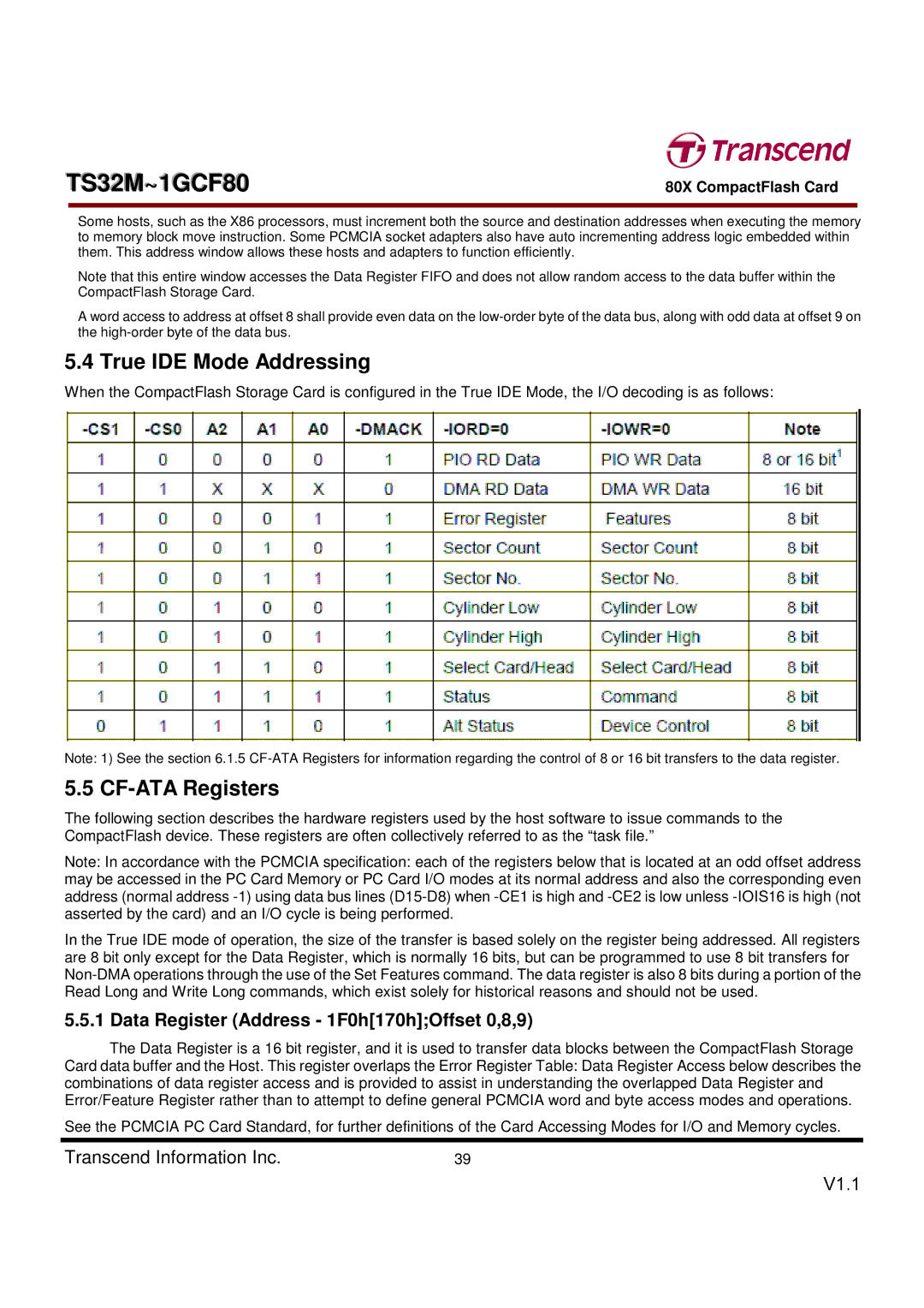
5.4 True IDE Mode Addressing
When the CompactFlash Storage Card is configured in the True IDE Mode, the I/O decoding is as follows:
Note: 1) See the section 6.1.5
5.5 CF-ATA Registers
The following section describes the hardware registers used by the host software to issue commands to the CompactFlash device. These registers are often collectively referred to as the “task file.”
Note: In accordance with the PCMCIA specification: each of the registers below that is located at an odd offset address may be accessed in the PC Card Memory or PC Card I/O modes at its normal address and also the corresponding even address (normal address
In the True IDE mode of operation, the size of the transfer is based solely on the register being addressed. All registers are 8 bit only except for the Data Register, which is normally 16 bits, but can be programmed to use 8 bit transfers for
5.5.1 Data Register (Address - 1F0h[170h];Offset 0,8,9)
The Data Register is a 16 bit register, and it is used to transfer data blocks between the CompactFlash Storage Card data buffer and the Host. This register overlaps the Error Register Table: Data Register Access below describes the combinations of data register access and is provided to assist in understanding the overlapped Data Register and Error/Feature Register rather than to attempt to define general PCMCIA word and byte access modes and operations.
See the PCMCIA PC Card Standard, for further definitions of the Card Accessing Modes for I/O and Memory cycles.
Transcend Information Inc. | 39 |