TS32M~1GCF80
4. Card Configuration
80X CompactFlash Card
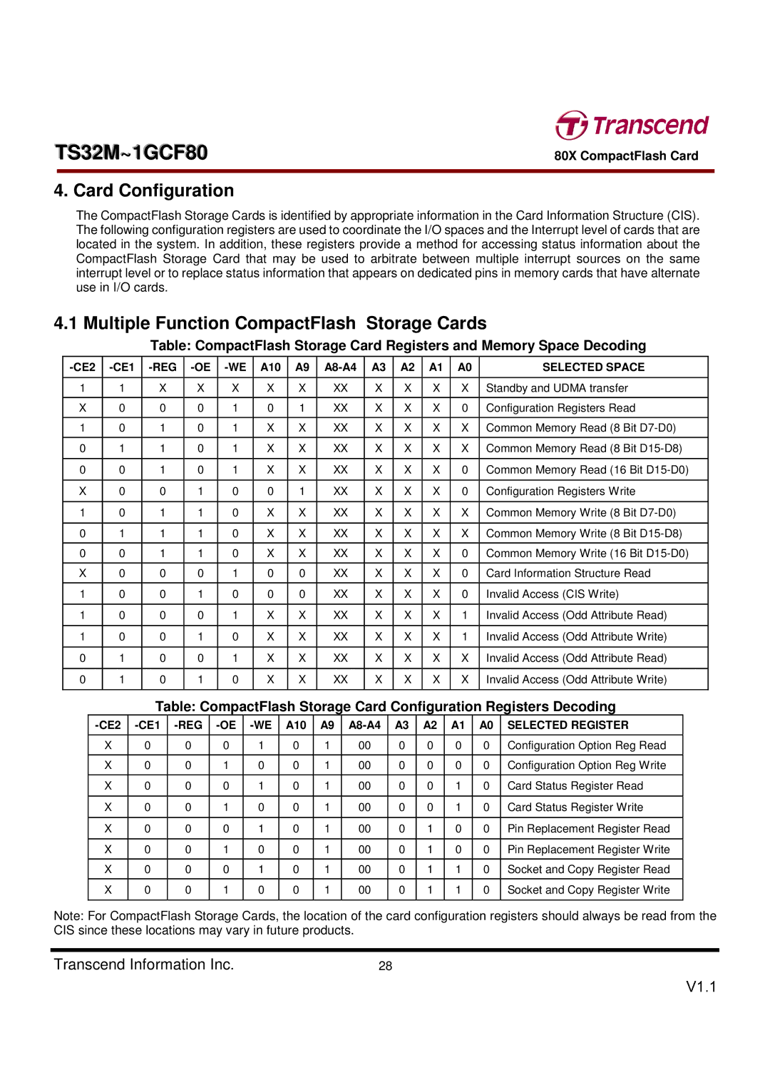
The CompactFlash Storage Cards is identified by appropriate information in the Card Information Structure (CIS). The following configuration registers are used to coordinate the I/O spaces and the Interrupt level of cards that are located in the system. In addition, these registers provide a method for accessing status information about the CompactFlash Storage Card that may be used to arbitrate between multiple interrupt sources on the same interrupt level or to replace status information that appears on dedicated pins in memory cards that have alternate use in I/O cards.
4.1 Multiple Function CompactFlash Storage Cards
Table: CompactFlash Storage Card Registers and Memory Space Decoding
|
| A10 | A9 |
| A3 | A2 | A1 | A0 | SELECTED SPACE | |||
|
|
|
|
|
|
|
|
|
|
|
|
|
1 | 1 | X | X | X | X | X | XX | X | X | X | X | Standby and UDMA transfer |
|
|
|
|
|
|
|
|
|
|
|
|
|
X | 0 | 0 | 0 | 1 | 0 | 1 | XX | X | X | X | 0 | Configuration Registers Read |
|
|
|
|
|
|
|
|
|
|
|
|
|
1 | 0 | 1 | 0 | 1 | X | X | XX | X | X | X | X | Common Memory Read (8 Bit |
|
|
|
|
|
|
|
|
|
|
|
|
|
0 | 1 | 1 | 0 | 1 | X | X | XX | X | X | X | X | Common Memory Read (8 Bit |
|
|
|
|
|
|
|
|
|
|
|
|
|
0 | 0 | 1 | 0 | 1 | X | X | XX | X | X | X | 0 | Common Memory Read (16 Bit |
|
|
|
|
|
|
|
|
|
|
|
|
|
X | 0 | 0 | 1 | 0 | 0 | 1 | XX | X | X | X | 0 | Configuration Registers Write |
|
|
|
|
|
|
|
|
|
|
|
|
|
1 | 0 | 1 | 1 | 0 | X | X | XX | X | X | X | X | Common Memory Write (8 Bit |
|
|
|
|
|
|
|
|
|
|
|
|
|
0 | 1 | 1 | 1 | 0 | X | X | XX | X | X | X | X | Common Memory Write (8 Bit |
|
|
|
|
|
|
|
|
|
|
|
|
|
0 | 0 | 1 | 1 | 0 | X | X | XX | X | X | X | 0 | Common Memory Write (16 Bit |
|
|
|
|
|
|
|
|
|
|
|
|
|
X | 0 | 0 | 0 | 1 | 0 | 0 | XX | X | X | X | 0 | Card Information Structure Read |
|
|
|
|
|
|
|
|
|
|
|
|
|
1 | 0 | 0 | 1 | 0 | 0 | 0 | XX | X | X | X | 0 | Invalid Access (CIS Write) |
|
|
|
|
|
|
|
|
|
|
|
|
|
1 | 0 | 0 | 0 | 1 | X | X | XX | X | X | X | 1 | Invalid Access (Odd Attribute Read) |
|
|
|
|
|
|
|
|
|
|
|
|
|
1 | 0 | 0 | 1 | 0 | X | X | XX | X | X | X | 1 | Invalid Access (Odd Attribute Write) |
|
|
|
|
|
|
|
|
|
|
|
|
|
0 | 1 | 0 | 0 | 1 | X | X | XX | X | X | X | X | Invalid Access (Odd Attribute Read) |
|
|
|
|
|
|
|
|
|
|
|
|
|
0 | 1 | 0 | 1 | 0 | X | X | XX | X | X | X | X | Invalid Access (Odd Attribute Write) |
|
|
|
|
|
|
|
|
|
|
|
|
|
Table: CompactFlash Storage Card Configuration Registers Decoding
A10 | A9 | A3 | A2 | A1 | A0 | SELECTED REGISTER | ||||||
|
|
|
|
|
|
|
|
|
|
|
|
|
X | 0 | 0 | 0 | 1 | 0 | 1 | 00 | 0 | 0 | 0 | 0 | Configuration Option Reg Read |
|
|
|
|
|
|
|
|
|
|
|
|
|
X | 0 | 0 | 1 | 0 | 0 | 1 | 00 | 0 | 0 | 0 | 0 | Configuration Option Reg Write |
|
|
|
|
|
|
|
|
|
|
|
|
|
X | 0 | 0 | 0 | 1 | 0 | 1 | 00 | 0 | 0 | 1 | 0 | Card Status Register Read |
|
|
|
|
|
|
|
|
|
|
|
|
|
X | 0 | 0 | 1 | 0 | 0 | 1 | 00 | 0 | 0 | 1 | 0 | Card Status Register Write |
|
|
|
|
|
|
|
|
|
|
|
|
|
X | 0 | 0 | 0 | 1 | 0 | 1 | 00 | 0 | 1 | 0 | 0 | Pin Replacement Register Read |
|
|
|
|
|
|
|
|
|
|
|
|
|
X | 0 | 0 | 1 | 0 | 0 | 1 | 00 | 0 | 1 | 0 | 0 | Pin Replacement Register Write |
|
|
|
|
|
|
|
|
|
|
|
|
|
X | 0 | 0 | 0 | 1 | 0 | 1 | 00 | 0 | 1 | 1 | 0 | Socket and Copy Register Read |
|
|
|
|
|
|
|
|
|
|
|
|
|
X | 0 | 0 | 1 | 0 | 0 | 1 | 00 | 0 | 1 | 1 | 0 | Socket and Copy Register Write |
|
|
|
|
|
|
|
|
|
|
|
|
|
Note: For CompactFlash Storage Cards, the location of the card configuration registers should always be read from the CIS since these locations may vary in future products.
Transcend Information Inc. | 28 |