130447-1 Rev. A
3.6.1 Control Processing
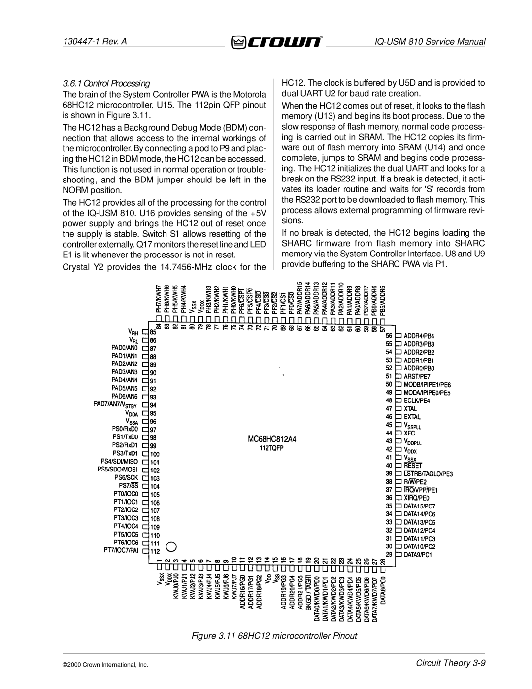
The brain of the System Controller PWA is the Motorola 68HC12 microcontroller, U15. The 112pin QFP pinout is shown in Figure 3.11.
The HC12 has a Background Debug Mode (BDM) con- nection that allows access to the internal workings of the microcontroller. By connecting a pod to P9 and plac- ing the HC12 in BDM mode, the HC12 can be accessed. This function is not used in normal operation or trouble- shooting, and the BDM jumper should be left in the NORM position.
The HC12 provides all of the processing for the control of the
Crystal Y2 provides the
HC12. The clock is buffered by U5D and is provided to dual UART U2 for baud rate creation.
When the HC12 comes out of reset, it looks to the flash memory (U13) and begins its boot process. Due to the slow response of flash memory, normal code process- ing is carried out in SRAM. The HC12 copies its firm- ware out of flash memory into SRAM (U14) and once complete, jumps to SRAM and begins code process- ing. The HC12 initializes the dual UART and looks for a break on the RS232 input. If a break is detected, it acti- vates its loader routine and waits for 'S' records from the RS232 port to be downloaded to flash memory. This process allows external programming of firmware revi- sions.
If no break is detected, the HC12 begins loading the SHARC firmware from flash memory into SHARC memory via the System Controller Interface. U8 and U9 provide buffering to the SHARC PWA via P1.
Figure 3.11 68HC12 microcontroller Pinout
©2000 Crown International, Inc.
Circuit Theory