|
|
3 Circuit Theory
3.1 Overview
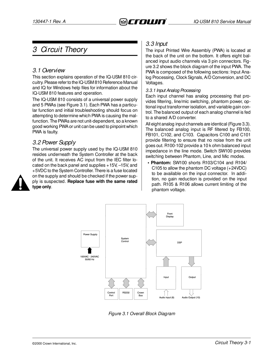
This section explains operation of the
The
3.2 Power Supply
The universal power supply used by the
3.3 Input
The input Printed Wire Assembly (PWA) is located at the back of the unit on the bottom. It offers eight bal- anced input audio channels via 3 pin connectors. Fig- ure 3.2 shows the block diagram of the input PWA. The PWA is composed of the following sections: Input Ana- log Processing, Clock Signals, A/D Conversion, and DC Voltages.
3.3.1 Input Analog Processing
Each input channel has analog processing that pro- vides filtering, line/mic switching, phantom power, op- tional input transformer isolation, and variable gain con- trol. The balanced output of each analog channel is fed to a shared A/D converter.
All eight analog input channels are identical (Figure 3.3). The balanced analog input is RF filtered by FB100, FB101, C102, and C103. Capacitors C100 and C101 provide filtering to ensure that no noise from the unit goes out.
•Phantom: SW100 shorts R103/C104 and R104/ C105 to allow the phantom DC voltage (+24VDC) to be available on the input connector. In addi- tion, no gain reduction is provided on the input path. R105 & R106 allows current limiting of the phantom voltage.
Figure 3.1 Overall Block Diagram
©2000 Crown International, Inc.
Circuit Theory
