Cypress CY7C0832BV Counter Reset Operation, Counter Load Operation, Counter Increment Operation

Models: CY7C0837AV CY7C0833AV CY7C0831AV CY7C0830AV CY7C0832AV CY7C0832BV

1 28
Download 28 pages 54.81 Kb
Page 7
Image 7

CY7C0837AV, CY7C0830AV CY7C0831AV, CY7C0832AV CY7C0832BV, CY7C0833AV

Counter Reset Operation

All unmasked bits of the counter are reset to ‘0.’ All masked bits remain unchanged. The mirror register is loaded with the value of the burst counter. A Mask Reset followed by a Counter Reset resets the counter and mirror registers to 00000, as does master reset (MRST).

Counter Load Operation

The address counter and mirror registers are both loaded with the address value presented at the address lines.

Counter Increment Operation

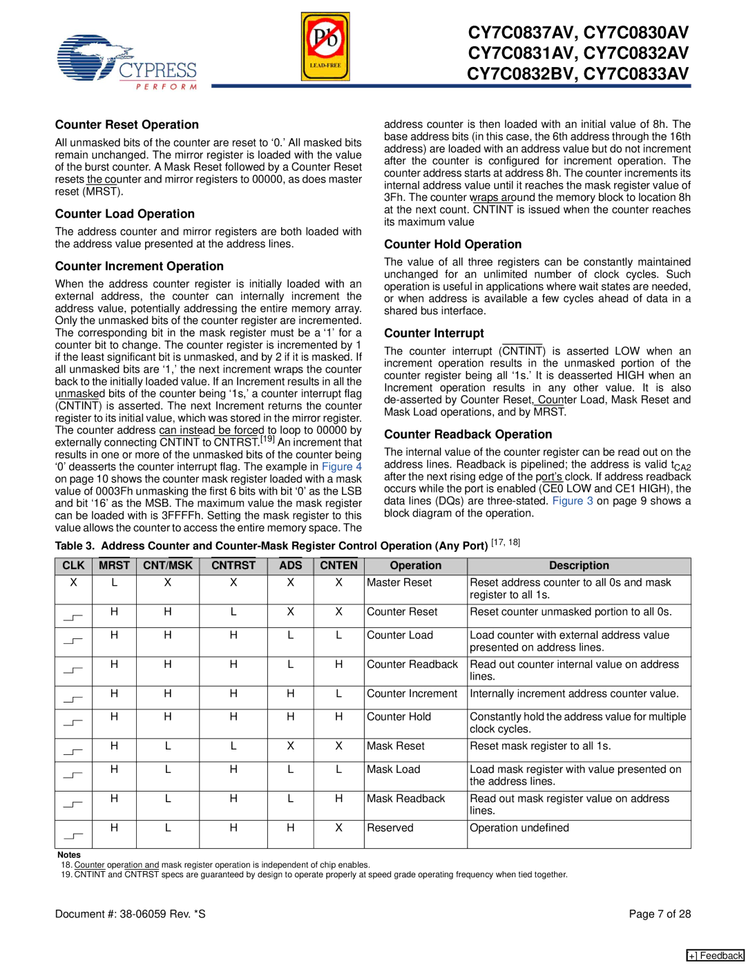
When the address counter register is initially loaded with an external address, the counter can internally increment the address value, potentially addressing the entire memory array. Only the unmasked bits of the counter register are incremented. The corresponding bit in the mask register must be a ‘1’ for a counter bit to change. The counter register is incremented by 1 if the least significant bit is unmasked, and by 2 if it is masked. If all unmasked bits are ‘1,’ the next increment wraps the counter back to the initially loaded value. If an Increment results in all the unmasked bits of the counter being ‘1s,’ a counter interrupt flag (CNTINT) is asserted. The next Increment returns the counter register to its initial value, which was stored in the mirror register. The counter address can instead be forced to loop to 00000 by externally connecting CNTINT to CNTRST.[19] An increment that results in one or more of the unmasked bits of the counter being ‘0’ deasserts the counter interrupt flag. The example in Figure 4 on page 10 shows the counter mask register loaded with a mask value of 0003Fh unmasking the first 6 bits with bit ‘0’ as the LSB and bit ‘16’ as the MSB. The maximum value the mask register can be loaded with is 3FFFFh. Setting the mask register to this value allows the counter to access the entire memory space. The

address counter is then loaded with an initial value of 8h. The base address bits (in this case, the 6th address through the 16th address) are loaded with an address value but do not increment after the counter is configured for increment operation. The counter address starts at address 8h. The counter increments its internal address value until it reaches the mask register value of 3Fh. The counter wraps around the memory block to location 8h at the next count. CNTINT is issued when the counter reaches its maximum value

Counter Hold Operation

The value of all three registers can be constantly maintained unchanged for an unlimited number of clock cycles. Such operation is useful in applications where wait states are needed, or when address is available a few cycles ahead of data in a shared bus interface.

Counter Interrupt

The counter interrupt (CNTINT) is asserted LOW when an increment operation results in the unmasked portion of the counter register being all ‘1s.’ It is deasserted HIGH when an Increment operation results in any other value. It is also de-asserted by Counter Reset, Counter Load, Mask Reset and Mask Load operations, and by MRST.

Counter Readback Operation

The internal value of the counter register can be read out on the address lines. Readback is pipelined; the address is valid tCA2 after the next rising edge of the port’s clock. If address readback occurs while the port is enabled (CE0 LOW and CE1 HIGH), the data lines (DQs) are three-stated. Figure 3 on page 9 shows a block diagram of the operation.

Table 3. Address Counter and Counter-Mask Register Control Operation (Any Port) [17, 18]

CLK

MRST

CNT/MSK

CNTRST

ADS

CNTEN

Operation

Description


X

L

X

X

X

X

Master Reset

Reset address counter to all 0s and mask


register to all 1s.


H

H

L

X

X

Counter Reset

Reset counter unmasked portion to all 0s.


H

H

H

L

L

Counter Load

Load counter with external address value


presented on address lines.


H

H

H

L

H

Counter Readback

Read out counter internal value on address


lines.


H

H

H

H

L

Counter Increment

Internally increment address counter value.


H

H

H

H

H

Counter Hold

Constantly hold the address value for multiple


clock cycles.


H

L

L

X

X

Mask Reset

Reset mask register to all 1s.


H

L

H

L

L

Mask Load

Load mask register with value presented on


the address lines.


H

L

H

L

H

Mask Readback

Read out mask register value on address


lines.


H

L

H

H

X

Reserved

Operation undefined


Notes

18.Counter operation and mask register operation is independent of chip enables.

19.CNTINT and CNTRST specs are guaranteed by design to operate properly at speed grade operating frequency when tied together.

Document #: 38-06059 Rev. *S

Page 7 of 28

[+] Feedback

Page 7
Image 7
Cypress CY7C0832BV Counter Reset Operation, Counter Load Operation, Counter Increment Operation, Counter Hold Operation

CY7C0837AV, CY7C0833AV, CY7C0831AV, CY7C0830AV, CY7C0832AV specifications

Cypress Semiconductor, a leader in innovative semiconductor solutions, has developed a range of high-performance SRAM (Static Random Access Memory) products, including the CY7C0837AV, CY7C0833AV, CY7C0831AV, CY7C0830AV, and CY7C0832AV. These devices cater to various applications requiring fast, reliable memory storage.

One of the main features of these SRAMs is their speed. They offer fast access times, which range from 10 to 15 nanoseconds. This rapid access is critical for applications where speed is essential, such as high-speed networking and telecommunications equipment, automotive systems, and industrial controls. The CY7C0837AV, for instance, boasts a 1 Mbit memory capacity, making it suitable for applications requiring a larger data buffer.

Another notable feature of these devices is their low power consumption. The SRAMs are designed to operate at low voltages, typically around 3.3V, which greatly reduces the overall power requirements. This characteristic is particularly advantageous for battery-operated devices and portable electronics, as it extends battery life and improves energy efficiency.

Cypress's SRAM offerings incorporate advanced technologies like asynchronous read and write operations, which enable users to access memory without the need for a clock signal. This asynchronous nature allows for simpler system designs and integration, significantly reducing component count and complexity.

In terms of packaging, these SRAMs are available in various formats, including standard DIP and surface-mount options, facilitating easy integration into a range of printed circuit boards. Their footprint and compatibility with existing designs ensure they can be utilized in both new developments and legacy system enhancements.

The CY7C0837AV, CY7C0833AV, CY7C0831AV, CY7C0830AV, and CY7C0832AV also support burst mode operations, allowing for faster sequential data access. This feature enhances performance in applications that require continuous data streams, such as video processing and signal processing tasks.

In summary, the Cypress CY7C0837AV, CY7C0833AV, CY7C0831AV, CY7C0830AV, and CY7C0832AV SRAMs provide a combination of high speed, low power consumption, and versatile packaging options. Their advanced technologies and characteristics make them ideal for a wide range of applications, from automotive to industrial systems, solidifying their position as reliable memory solutions in the semiconductor market.