|
|
|
| CY7C1361C | |
|
|
|
| CY7C1363C | |
|
|
|
| ||
|
|
|
|
|
|
|
|
|
|
|
|
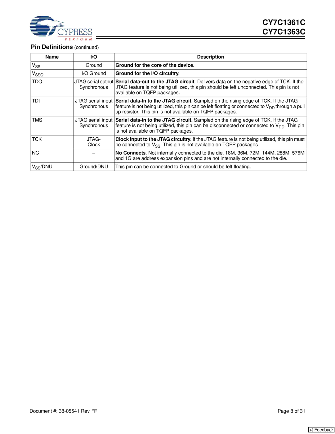
Pin Definitions (continued) |
|
| |||
|
|
| |||
Name | I/O | Description | |||
|
|
| |||
VSS | Ground | Ground for the core of the device. | |||
VSSQ | I/O Ground | Ground for the I/O circuitry. | |||
TDO | JTAG serial output | Serial | |||
| Synchronous | JTAG feature is not being utilized, this pin should be left unconnected. This pin is not | |||
|
|
|
| available on TQFP packages. | |
TDI | JTAG serial input | Serial | |||
| Synchronous | feature is not being utilized, this pin can be left floating or connected to VDD through a pull | |||
|
|
|
| up resistor. This pin is not available on TQFP packages. | |
TMS | JTAG serial input | Serial | |||
| Synchronous | feature is not being utilized, this pin can be disconnected or connected to VDD. This pin | |||
|
|
|
| is not available on TQFP packages. | |
TCK | JTAG- | Clock input to the JTAG circuitry. If the JTAG feature is not being utilized, this pin must | |||
| Clock | be connected to VSS. This pin is not available on TQFP packages. | |||
NC | – | No Connects. Not internally connected to the die. 18M, 36M, 72M, 144M, 288M, 576M | |||
|
|
|
| and 1G are address expansion pins and are not internally connected to the die. | |
VSS/DNU | Ground/DNU | This pin can be connected to Ground or should be left floating. | |||
Document #: | Page 8 of 31 |
[+] Feedback