CY7C1474V25, CY7C1470V25, CY7C1472V25 specifications
The Cypress CY7C1470V25, CY7C1474V25, and CY7C1472V25 are part of Cypress Semiconductor’s family of high-performance synchronous static random-access memory (SRAM) solutions. These memory devices are designed specifically for applications that require fast access times and high bandwidth, making them ideal for a variety of consumer and industrial applications.One of the standout features of these SRAMs is their performance. They provide high-speed access times, with data transfer rates that can reach up to 1 GHz. This performance is particularly beneficial for high-speed applications including networking equipment, telecommunications, and video processing systems. The CY7C1470V25, for example, offers a 256K x 16 configuration with an access time as low as 3.5 ns. Similarly, the CY7C1474V25 and CY7C1472V25 variants provide respective memory sizes of 1M x 16 and 512K x 16, catering to diverse memory application needs.
These SRAMs utilize a synchronous interface, which provides greater control over data transfers and synchronization with external clock signals. This synchronous operation allows for more efficient data handling in high-speed environments, reducing latency and improving system performance overall.
In terms of power consumption, the Cypress CY7C147x series is designed to operate efficiently. With a low operating voltage of 2.5V, these devices minimize energy usage while still delivering high-speed performance. The low standby power makes them suitable for battery-operated devices, as well as for systems where energy efficiency is a priority.
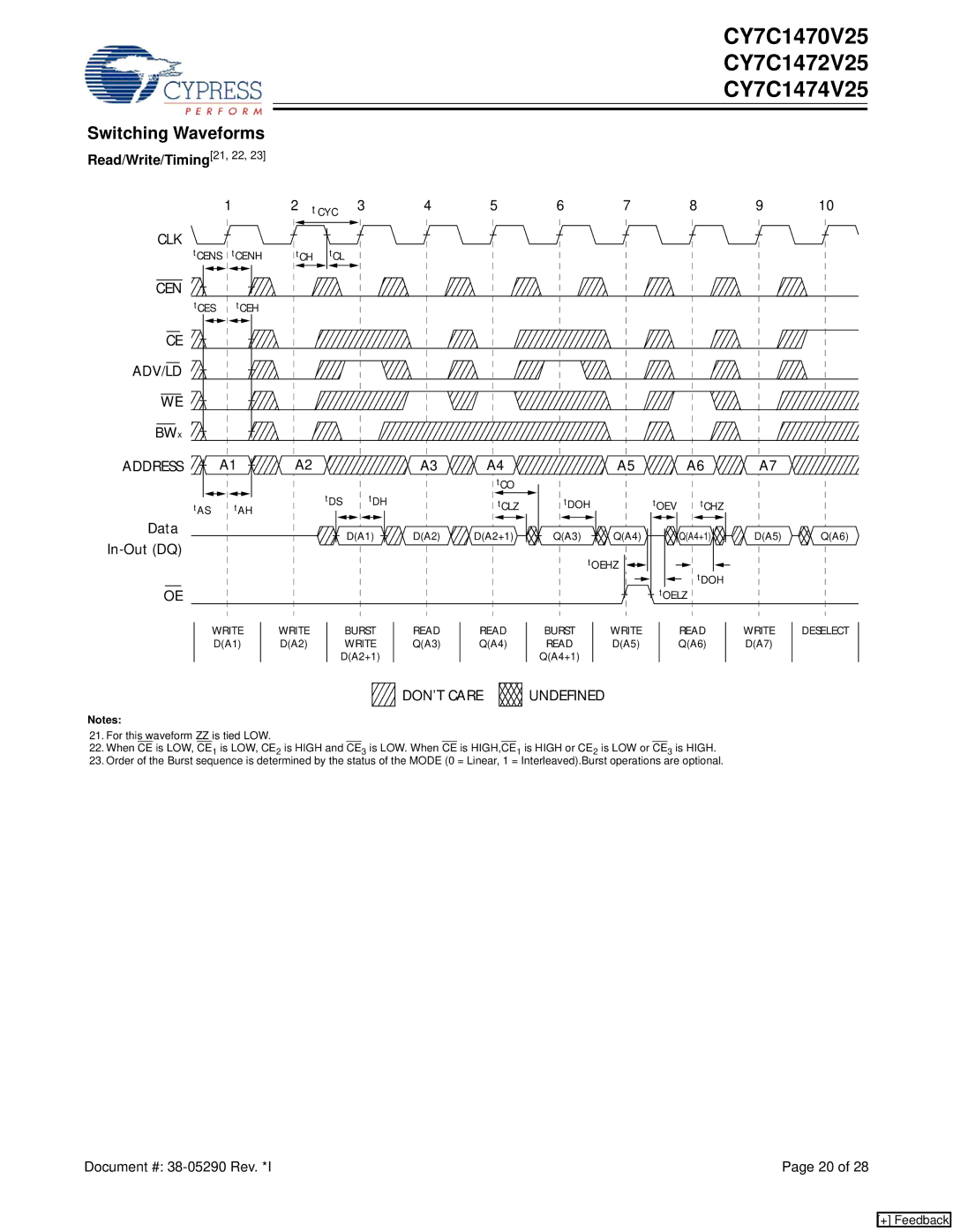
Furthermore, these SRAMs come with built-in features such as burst mode, which allows for sequential data access, enhancing read and write operations. This is especially useful in applications requiring rapid data retrieval.
The packaging options for the CY7C1470V25, CY7C1474V25, and CY7C1472V25 include both fine-pitch ball grid array (FBGA) and other configurations, facilitating easy integration into various circuit board layouts.
In conclusion, the Cypress CY7C1470V25, CY7C1474V25, and CY7C1472V25 SRAMs are powerful memory solutions that combine high-speed performance, low power consumption, and a synchronous interface. Their robust design makes them suitable for a wide array of applications ranging from communications to consumer electronics, ensuring they meet the demands of modern technology.

