|
|
|
|
|
|
|
| CY7C604XX |
|
|
|
|
|
|
|
|
|
|
|
|
|
|
|
|
| |
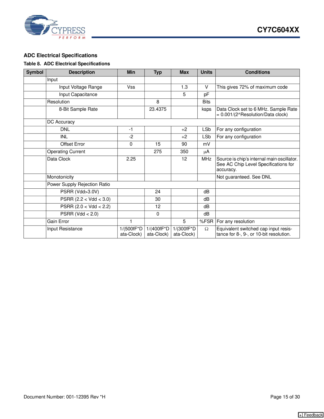
ADC Electrical Specifications |
|
|
|
|
| |||
Table 8. ADC Electrical Specifications |
|
|
|
|
| |||
|
|
|
|
|
|
| ||
Symbol | Description | Min | Typ | Max | Units | Conditions | ||
| Input |
|
|
|
|
| ||
|
|
|
|
|
|
| ||
| Input Voltage Range | Vss |
| 1.3 | V | This gives 72% of maximum code | ||
|
|
|
|
|
|
| ||
| Input Capacitance |
|
| 5 | pF |
| ||
|
|
|
|
|
|
| ||
| Resolution |
| 8 |
| Bits |
| ||
|
|
|
|
|
|
| ||
|
| 23.4375 |
| ksps | Data Clock set to 6 MHz. Sample Rate | |||
|
|
|
|
|
|
|
| = 0.001/(2^Resolution/Data clock) |
| DC Accuracy |
|
|
|
|
| ||
|
|
|
|
|
|
| ||
| DNL |
| +2 | LSb | For any configuration | |||
|
|
|
|
|
|
| ||
| INL |
| +2 | LSb | For any configuration | |||
|
|
|
|
|
|
| ||
| Offset Error | 0 | 15 | 90 | mV |
| ||
|
|
|
|
|
|
| ||
| Operating Current |
| 275 | 350 | μA |
| ||
|
|
|
|
|
|
| ||
| Data Clock | 2.25 |
| 12 | MHz | Source is chip’s internal main oscillator. | ||
|
|
|
|
|
|
|
| See AC Chip Level Specifications for |
|
|
|
|
|
|
|
| accuracy. |
| Monotonicity |
|
|
|
| Not guaranteed. See DNL | ||
|
|
|
|
|
|
| ||
| Power Supply Rejection Ratio |
|
|
|
|
| ||
|
|
|
|
|
|
| ||
| PSRR (Vdd>3.0V) |
| 24 |
| dB |
| ||
|
|
|
|
|
|
| ||
| PSRR (2.2 < Vdd < 3.0) |
| 30 |
| dB |
| ||
|
|
|
|
|
|
| ||
| PSRR (2.0 < Vdd < 2.2) |
| 12 |
| dB |
| ||
|
|
|
|
|
|
| ||
| PSRR (Vdd < 2.0) |
| 0 |
| dB |
| ||
|
|
|
|
|
|
| ||
| Gain Error | 1 |
| 5 | %FSR | For any resolution | ||
|
|
|
|
|
|
| ||
| Input Resistance | 1/(500fF*D | 1/(400fF*D | 1/(300fF*D | Ω | Equivalent switched cap input resis- | ||
|
|
|
|
| tance for | |||
Document Number: | Page 15 of 30 |
[+] Feedback