CY7C604XX
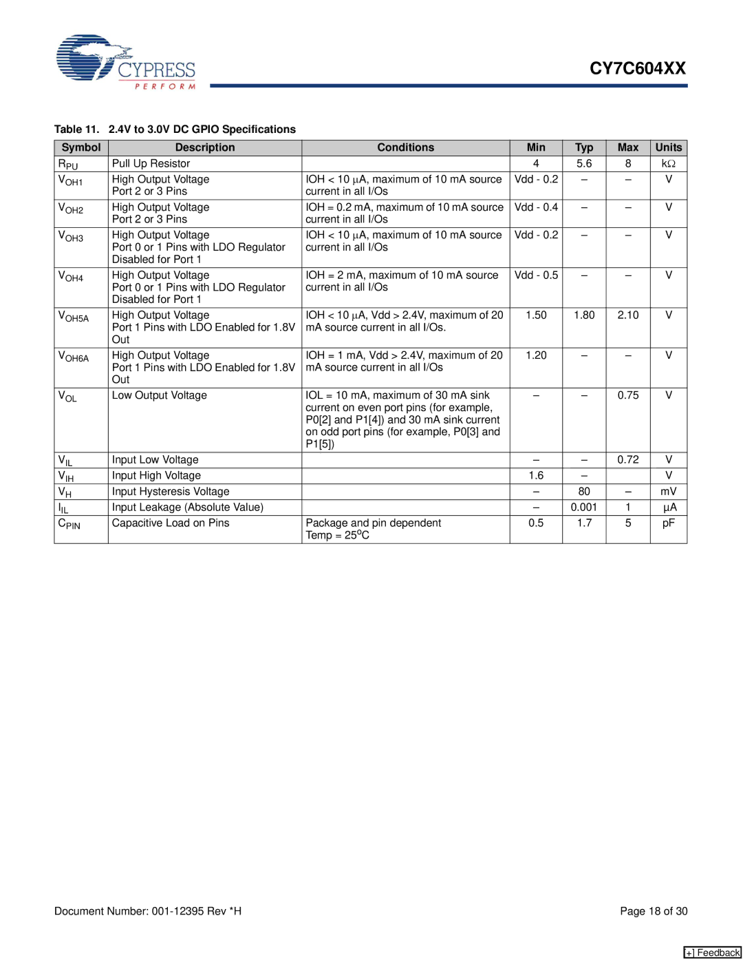
Table 11. 2.4V to 3.0V DC GPIO Specifications
Symbol | Description | Conditions | Min | Typ | Max | Units |
RPU | Pull Up Resistor |
| 4 | 5.6 | 8 | kΩ |
VOH1 | High Output Voltage | IOH < 10 μA, maximum of 10 mA source | Vdd - 0.2 | – | – | V |
| Port 2 or 3 Pins | current in all I/Os |
|
|
|
|
VOH2 | High Output Voltage | IOH = 0.2 mA, maximum of 10 mA source | Vdd - 0.4 | – | – | V |
| Port 2 or 3 Pins | current in all I/Os |
|
|
|
|
VOH3 | High Output Voltage | IOH < 10 μA, maximum of 10 mA source | Vdd - 0.2 | – | – | V |
| Port 0 or 1 Pins with LDO Regulator | current in all I/Os |
|
|
|
|
| Disabled for Port 1 |
|
|
|
|
|
VOH4 | High Output Voltage | IOH = 2 mA, maximum of 10 mA source | Vdd - 0.5 | – | – | V |
| Port 0 or 1 Pins with LDO Regulator | current in all I/Os |
|
|
|
|
| Disabled for Port 1 |
|
|
|
|
|
VOH5A | High Output Voltage | IOH < 10 μA, Vdd > 2.4V, maximum of 20 | 1.50 | 1.80 | 2.10 | V |
| Port 1 Pins with LDO Enabled for 1.8V | mA source current in all I/Os. |
|
|
|
|
| Out |
|
|
|
|
|
VOH6A | High Output Voltage | IOH = 1 mA, Vdd > 2.4V, maximum of 20 | 1.20 | – | – | V |
| Port 1 Pins with LDO Enabled for 1.8V | mA source current in all I/Os |
|
|
|
|
| Out |
|
|
|
|
|
VOL | Low Output Voltage | IOL = 10 mA, maximum of 30 mA sink | – | – | 0.75 | V |
|
| current on even port pins (for example, |
|
|
|
|
|
| P0[2] and P1[4]) and 30 mA sink current |
|
|
|
|
|
| on odd port pins (for example, P0[3] and |
|
|
|
|
|
| P1[5]) |
|
|
|
|
VIL | Input Low Voltage |
| – | – | 0.72 | V |
VIH | Input High Voltage |
| 1.6 | – |
| V |
VH | Input Hysteresis Voltage |
| – | 80 | – | mV |
IIL | Input Leakage (Absolute Value) |
| – | 0.001 | 1 | µA |
CPIN | Capacitive Load on Pins | Package and pin dependent | 0.5 | 1.7 | 5 | pF |
|
| Temp = 25oC |
|
|
|
|
Document Number: | Page 18 of 30 |
[+] Feedback